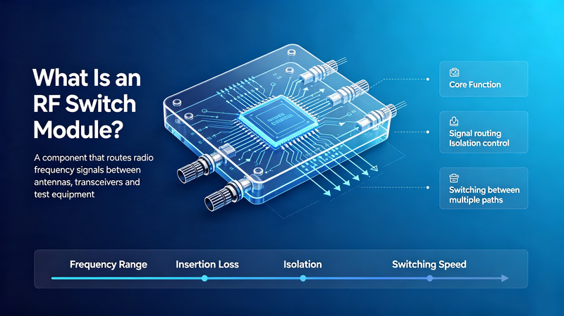


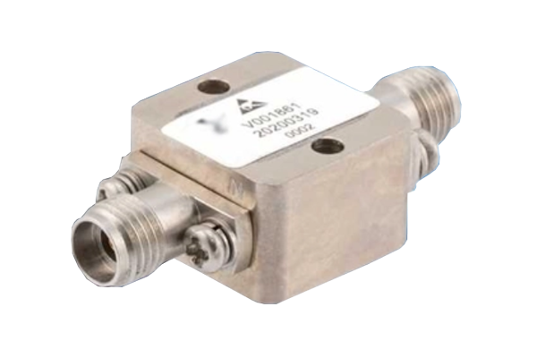
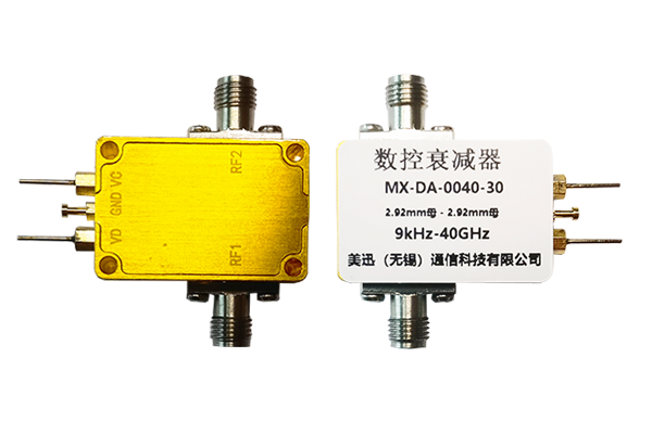
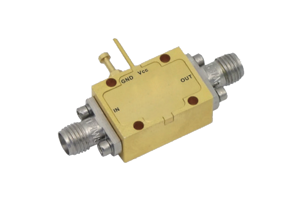
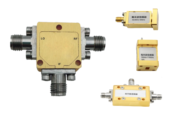




An RF switch circuit diagram provides a visual representation of how radio frequency signals are routed, controlled, and isolated within an RF system. RF switches are essential components used in wireless communication, radar systems, satellite links, test equipment, and microwave applications.
Understanding an RF switch circuit diagram helps engineers select suitable switch architectures, optimize signal performance, and design reliable high-frequency systems.
What Is an RF Switch Circuit Diagram?
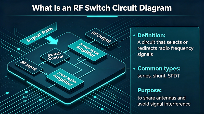
An RF switch circuit diagram illustrates the electrical connection between RF input ports, output ports, switching devices, control circuits, and bias networks. Unlike conventional low-frequency switches, RF switches must maintain signal integrity at high frequencies while minimizing insertion loss, VSWR, and signal distortion.
A typical RF switch circuit diagram includes:
- RF input and output transmission lines
- Switching elements such as PIN diodes, FETs, MEMS, or electromechanical contacts
- DC control circuits
- Bias networks and isolation components
- Matching circuits for impedance control
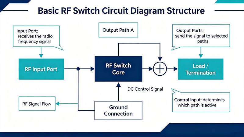
Basic RF Switch Circuit Diagram Structure
│
│
┌───────────────┐
│ RF Switching │
│ Element │
└───────────────┘
│
┌────────┬────────┐
│ │ │
RF OUT1 RF OUT2 RF OUT3
Control Signal → Bias Circuit → Switch Driver
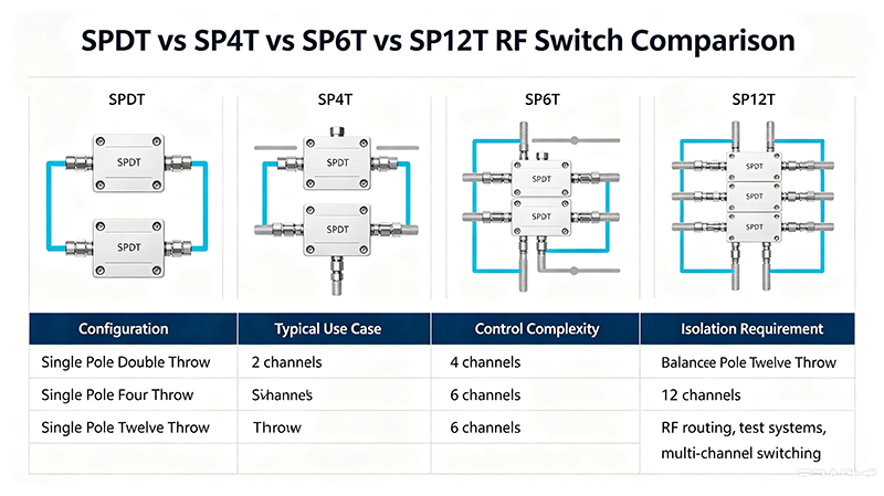
The circuit above represents a basic SPDT RF switch configuration, where one input signal can be connected to one of two output channels. More advanced configurations such as SP4T, SP6T, and SP12T RF switches use multiple switching paths to support complex RF routing.
Main Components in an RF Switch Circuit
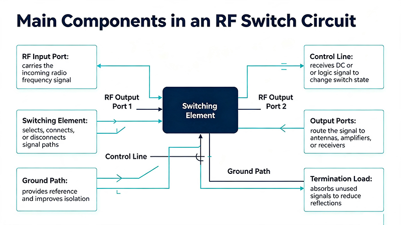
1. RF Switching Element
The switching element determines the performance characteristics of the RF switch. Different technologies provide different advantages depending on frequency range, power handling, switching speed, and reliability requirements.
| Switch Technology | Working Principle | Main Advantages |
|---|---|---|
| PIN Diode Switch | Uses diode bias control to change RF signal paths | High frequency capability, fast switching |
| FET RF Switch | Controls signal flow using semiconductor channels | Compact size and low power consumption |
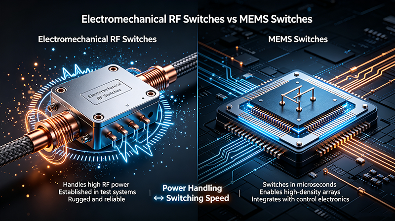
| MEMS Switch | Uses mechanical movement at microscopic scale | Low insertion loss and excellent isolation |
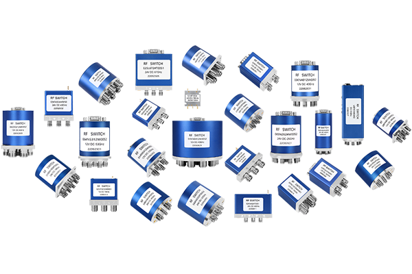
| Electromechanical RF Switch | Uses physical contacts for signal routing | High power handling and reliability |
2. Control and Bias Circuit
The control circuit provides the required voltage or current to activate the RF switching element. For example, PIN diode RF switches require forward or reverse bias conditions to control signal transmission.
A properly designed bias network prevents RF leakage into the control circuit while ensuring stable switching performance.
3. Transmission Line Structure
At microwave frequencies, PCB traces behave as transmission lines rather than simple conductors. RF switch circuit diagrams must consider characteristic impedance, usually 50 ohms, to prevent signal reflection and power loss.
How Does an RF Switch Circuit Work?
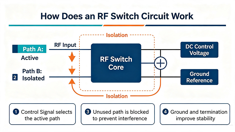
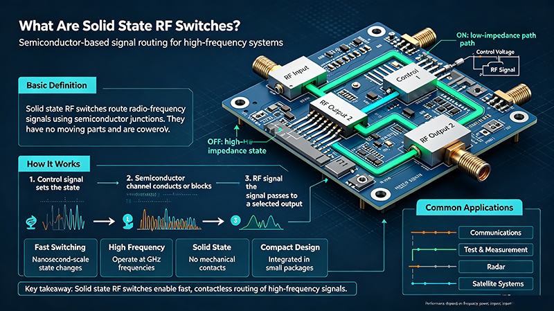
The operation of an RF switch depends on the selected switching technology. In a typical semiconductor RF switch, the control signal changes the state of the switching device, allowing the RF signal to pass through one path while isolating another path.
Signal Switching Process:
- The control system sends a switching command.
- The bias circuit applies the required voltage or current.
- The RF switching element changes its impedance state.
- The RF signal is routed to the selected output port.
- The unused path remains isolated to reduce interference.
RF Switch Circuit Diagram Types
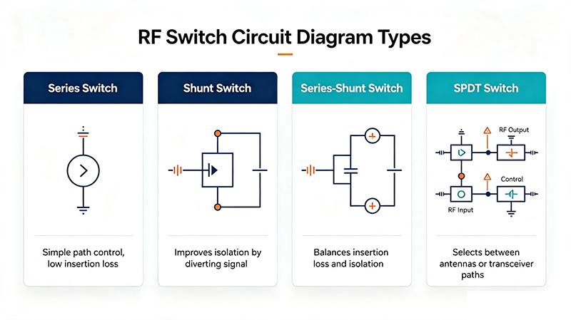
SPST RF Switch Circuit
An SPST (Single Pole Single Throw) RF switch provides simple ON/OFF signal control. It is commonly used for antenna switching, signal blocking, and RF protection circuits.
SPDT RF Switch Circuit
An SPDT (Single Pole Double Throw) RF switch connects one input signal to two possible output paths. This configuration is widely used in RF transceivers and measurement systems.
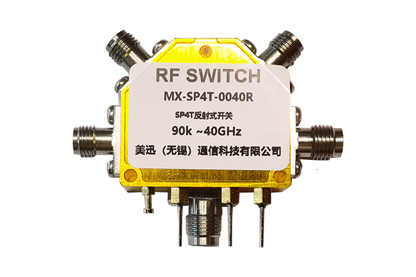
SP4T and Multi-Throw RF Switch Circuits
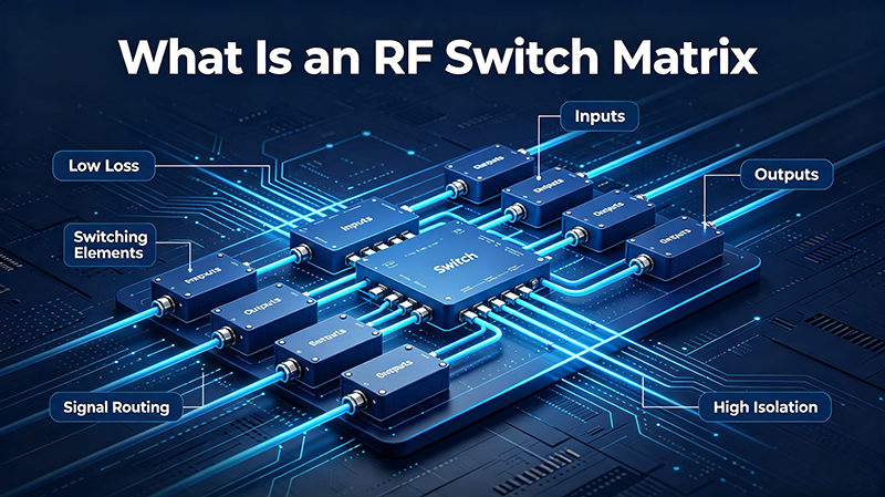
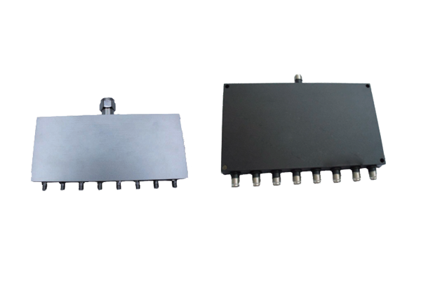
Multi-throw RF switches allow one RF input to connect with multiple outputs. They are frequently used in communication systems requiring multiple frequency bands or antenna paths.
Key RF Switch Circuit Design Considerations
- Insertion Loss: Lower insertion loss improves overall system efficiency and signal strength.
- Isolation: High isolation prevents unwanted signal coupling between channels.
- VSWR: Low VSWR ensures better impedance matching and reduces signal reflection.
- Power Handling: The circuit must withstand the maximum RF input power.
- Switching Speed: Fast switching is important for radar and communication applications.
Applications of RF Switch Circuits
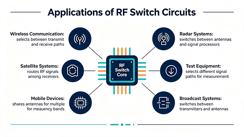
RF switch circuits are widely used across many industries:
- 5G base stations and wireless communication systems
- Radar transmit and receive modules
- Satellite communication equipment
- RF test and measurement systems
- Electronic warfare systems
- Antenna switching networks
- Microwave instrumentation
How to Choose the Right RF Switch Circuit Design
Selecting the correct RF switch circuit requires evaluating frequency range, power level, switching speed, control method, and environmental conditions.
Engineers should analyze:
- Operating frequency requirements
- Maximum RF power level
- Required number of ports
- Acceptable insertion loss
- Required isolation performance
- Mechanical and environmental requirements
Conclusion
An RF switch circuit diagram is an important tool for understanding how high-frequency signals are controlled and routed in modern electronic systems. From simple SPST switches to complex multi-port microwave switching networks, proper circuit design directly impacts signal quality, reliability, and system performance.
By understanding switching components, control circuits, transmission line design, and key RF parameters, engineers can develop optimized RF switch solutions for communication, radar, testing, and aerospace applications.