

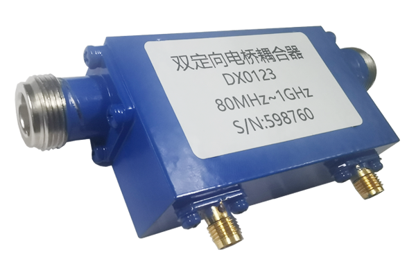
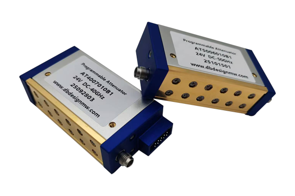
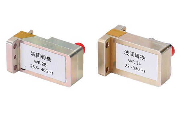
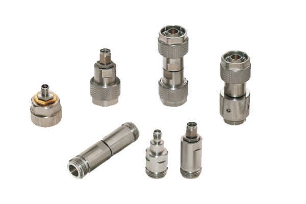
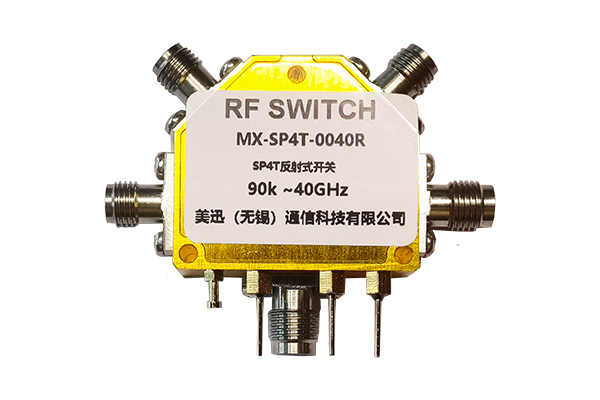
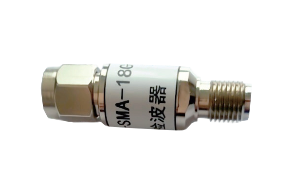
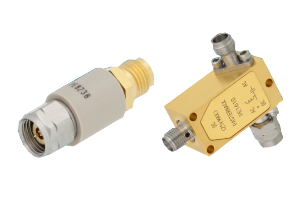
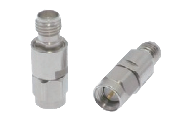
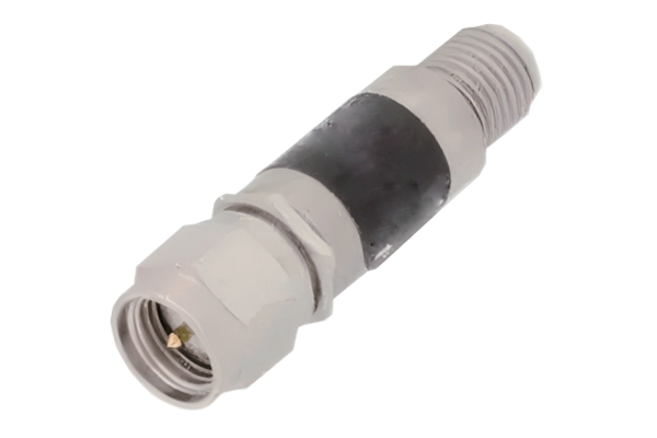
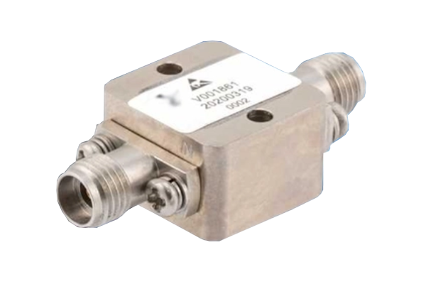
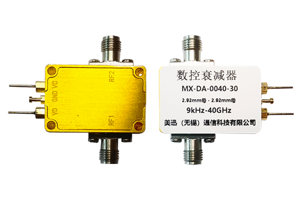
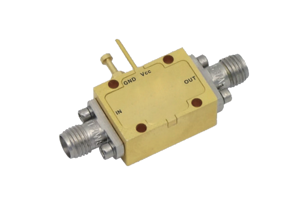
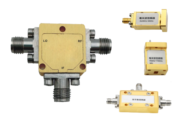




RF switches are fundamental components in virtually every wireless communication system. From smartphones to radar, satellite communications to test equipment, these versatile devices control signal routing with precision and reliability. This comprehensive guide explains what RF switches are, how they work, and why they are essential in modern electronics.
What is an RF Switch?
Definition
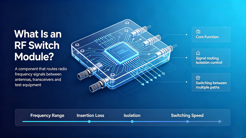
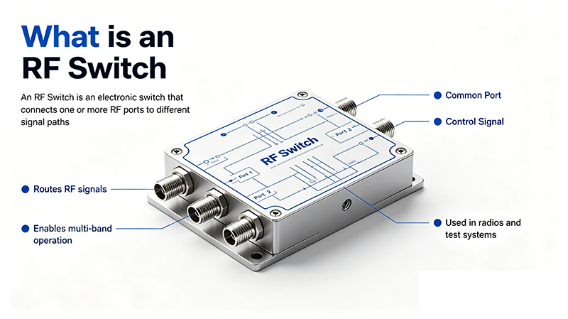
An RF (Radio Frequency) switch is an electronic component that controls the routing of high-frequency signals between different paths in a circuit. Operating typically from DC to 100+ GHz, these switches can connect or disconnect signal paths, select between multiple inputs or outputs, and direct RF signals with minimal loss and distortion.
RF switches serve as the "traffic controllers" of radio frequency systems. They enable devices to change signal paths quickly, switch between antennas, select different filters, alternate between transmit and receive modes, and perform many other critical functions that make modern wireless communications possible.
Unlike traditional electrical switches, RF switches must maintain precise 50-ohm (or other specified) impedance throughout the signal path to minimize signal reflections and preserve signal integrity. They are designed specifically to handle the unique challenges of high-frequency signals, including skin effect losses, parasitic reactances, and electromagnetic interference.
Primary Functions of RF Switches
- Signal Routing: Direct RF signals between different circuit paths
- Path Selection: Choose between multiple antennas, filters, or amplifiers
- T/R Switching: Alternate between transmit and receive modes
- Band Selection: Switch between different frequency bands
- Redundancy Switching: Provide backup paths for critical applications
- Test Routing: Connect test equipment to devices under test
How Does an RF Switch Work?
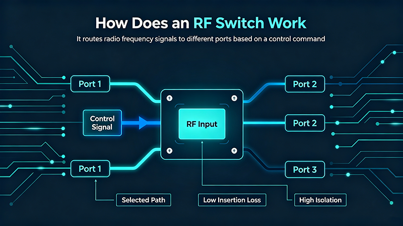
RF switches operate by controlling the electrical connection between input and output ports using either electromechanical or solid-state mechanisms. The basic principle involves creating a low-loss path (ON state) or a high-isolation barrier (OFF state) between signal ports.
Working Principle: Electromechanical Switches
Electromechanical RF switches use physical movement of contacts to route signals:
- A control voltage energizes an electromagnetic coil or actuator
- The actuator physically moves RF contacts between positions
- When contacts touch, they create a low-resistance path for RF signals
- When contacts separate, they block RF signal transmission
- A spring mechanism returns contacts to default position when de-energized
Working Principle: Solid-State Switches
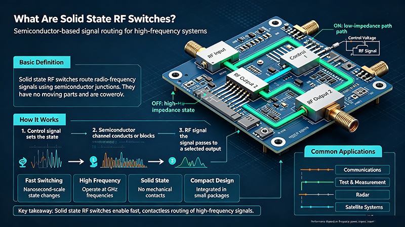
Solid-state RF switches use semiconductor devices to control signal flow without moving parts:
- A control voltage biases the semiconductor devices (FET, PIN diode, etc.)
- Forward bias creates a low-impedance path that allows signals to pass
- Reverse bias creates a high-impedance path that blocks signals
- The bias state determines whether the switch is ON or OFF
- Switching happens at electronic speeds (nanoseconds to microseconds)
Switch Configurations
RF switches are available in several configurations:
| Configuration | Description | Common Use |
|---|---|---|
| SPST | Single-Pole Single-Throw (1 input, 1 output, ON/OFF) | Simple signal blocking |
| SPDT | Single-Pole Double-Throw (1 input, 2 outputs) | T/R switching, source selection |
| SP3T-SP6T | Single-Pole Multi-Throw (1 input, 3-6 outputs) | Multi-band selection, antenna diversity |
| DPDT | Double-Pole Double-Throw (2 inputs, 2 outputs) | Differential switching, redundancy |
| Matrix | Multiple inputs to multiple outputs | Test equipment, complex routing |
Key Operational Insight
The most common RF switch configuration is SPDT (Single-Pole Double-Throw), which routes one input signal to one of two outputs. This configuration is fundamental to T/R (transmit/receive) switching in radar and communication systems.
Types of RF Switches
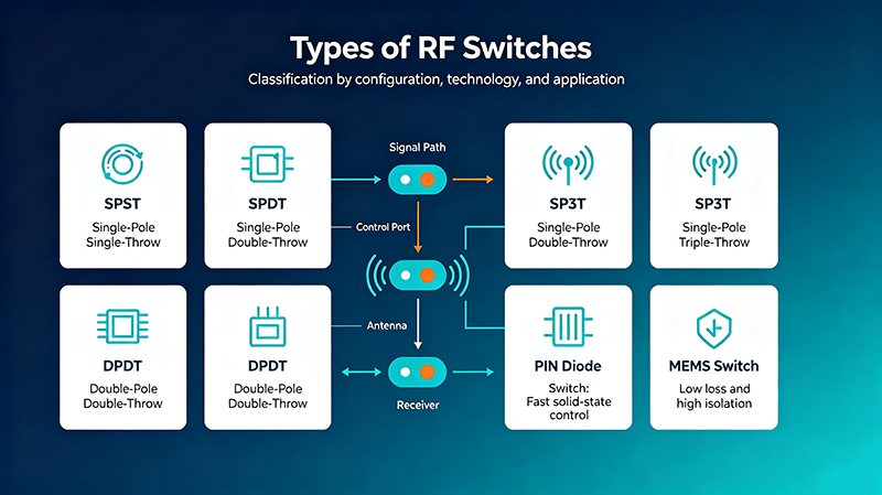
RF switches are categorized by their switching mechanism, each offering different advantages for specific applications.
Electromechanical Switches
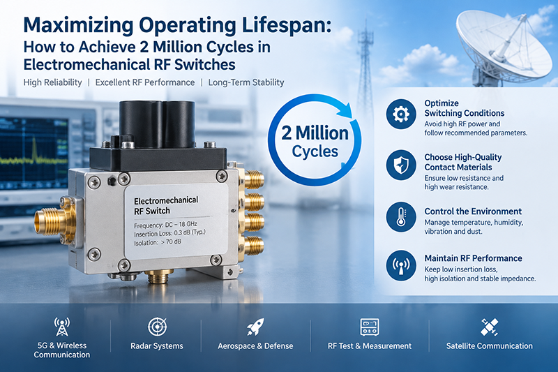
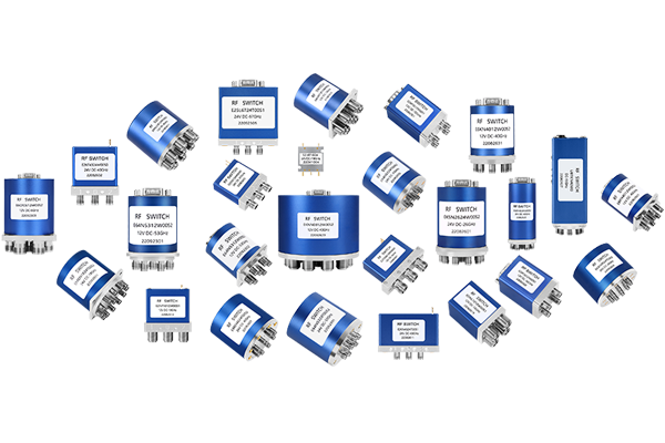
Use physical relay contacts moved by electromagnetic actuators. Excellent isolation, high power handling, but slower switching and limited mechanical life.
Solid-State Switches
Use semiconductor devices (PIN diodes, FETs) for switching. Fast switching, long life, silent operation, but lower power handling than electromechanical.
PIN Diode Switches
Specific type of solid-state switch using PIN diodes. Excellent for high-frequency applications with good linearity and fast switching.
FET Switches
Use GaAs or CMOS FETs for switching. Very fast switching, low power consumption, ideal for integrated circuits and mobile devices.
RF MEMS Switches
Micro-electromechanical systems combining mechanical switching with semiconductor fabrication. Low loss, high isolation, excellent for high-frequency applications.
Coaxial Switches
Electromechanical switches with coaxial connectors for easy integration. Common in test equipment and high-power applications.
Technology Comparison
| Technology | Speed | Isolation | Power Handling | Lifetime | Best For |
|---|---|---|---|---|---|
| Electromechanical | 5-15 ms | 60-90 dB | Up to 500W | 10^6-10^7 cycles | Test, high power |
| PIN Diode | 1-100 ns | 30-50 dB | Up to 50W | 10^10+ cycles | Radar, fast switching |
| GaAs FET | 1-10 ns | 40-60 dB | Up to 10W | 10^10+ cycles | Mobile, integrated |
| RF MEMS | 1-10 us | 50-80 dB | Up to 5W | 10^8-10^9 cycles | High-frequency, low loss |
Key RF Switch Specifications
Understanding RF switch specifications is essential for proper component selection. Here are the most important parameters:
Primary Specifications
1. Frequency Range
The operating frequency range over which the switch maintains acceptable performance. Modern RF switches cover from DC to 100+ GHz, with specific ranges optimized for different applications.
2. Insertion Loss
The signal power lost when passing through the switch in the ON state. Measured in decibels (dB), lower values indicate better performance. Typical values range from 0.2 to 2.5 dB depending on technology and frequency.
3. Isolation
The amount of signal blocked between ports when the switch is in the OFF state. Higher isolation is better, with values typically ranging from 30 to 90 dB. Critical for preventing signal leakage in sensitive applications.
4. VSWR (Voltage Standing Wave Ratio)
Measures impedance matching quality. Lower VSWR (closer to 1:1) indicates better matching and less signal reflection. Typically specified as less than 1.5:1 for quality switches.
5. Power Handling
The maximum RF power the switch can handle without damage or performance degradation. Specified separately for CW (continuous wave) and peak power. Critical consideration for transmitter applications.
6. Switching Speed
The time required for the switch to change state. Measured from control signal change to stable RF output. Critical for time-sensitive applications like radar and frequency hopping systems.
Secondary Specifications
- IP3 (Third-Order Intercept Point): Measures linearity and intermodulation performance
- P1dB (1dB Compression Point): Indicates when gain compression begins
- Control Voltage/Current: Required drive signals for switching
- Operating Temperature: Range over which specifications are maintained
- MTBF (Mean Time Between Failures): Reliability specification
- Connector Type: Physical interface specification (SMA, N-Type, etc.)
Common Applications of RF Switches
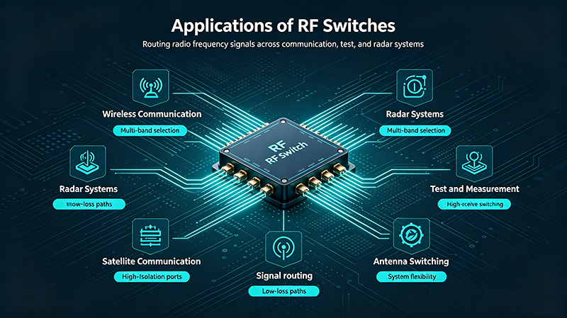
Where Are RF Switches Used?
RF switches are ubiquitous in modern wireless systems, serving critical functions across virtually every application that involves radio frequency signals.
5G and Cellular Networks
Base stations use RF switches for transmit/receive switching, band selection, and antenna beamforming. Mobile devices use them for antenna switching and carrier aggregation.
Radar Systems
Phased array radars contain thousands of T/R switches for beam steering. Weather and military radars rely on switches for rapid signal routing.
Satellite Communications
Ground stations and satellite transponders use RF switches for redundancy, polarization selection, and beam routing in communication systems.
Test and Measurement
Network analyzers, spectrum analyzers, and automated test equipment use RF switches to route signals between multiple test ports and DUTs.
Automotive Electronics
Modern vehicles use RF switches in infotainment systems, keyless entry, V2X communications, and increasingly in automotive radar for safety systems.
IoT and Smart Devices
Wi-Fi routers, Bluetooth devices, smart home products, and industrial sensors all incorporate RF switches for efficient signal management.
Electronic Warfare
Military EW systems use RF switches for threat detection, jamming signal generation, and protective countermeasures against enemy RF signals.
Medical Equipment
MRI machines, medical imaging systems, and wireless patient monitoring use RF switches for signal routing in critical diagnostic applications.
Advantages and Trade-offs
Different RF switch technologies offer distinct advantages and limitations. Understanding these trade-offs helps in selecting the right switch for your application.
Electromechanical vs Solid-State
Electromechanical Advantages
- Excellent isolation (60-90 dB)
- High power handling (up to 500W)
- Low insertion loss (0.2-0.5 dB)
- Wide frequency range
- Good linearity performance
- DC to high frequency coverage
Solid-State Advantages
- Fast switching (nanoseconds)
- Long operational life
- Silent operation
- Compact size
- Low power consumption
- High reliability
- No moving parts
Common Trade-offs
| Trade-off | Description | Best Solution |
|---|---|---|
| Speed vs Isolation | Faster switching often means lower isolation | Choose based on system priorities |
| Power vs Speed | Higher power handling typically slower | Match switch to signal levels |
| Frequency vs Performance | Higher frequencies reduce all specs | Select narrowband for best results |
| Cost vs Performance | Better specs increase cost | Optimize for system requirements |
Future Trends
Emerging technologies like RF MEMS are combining the best of electromechanical and solid-state approaches, offering low loss with fast switching. Integration with control electronics and digital interfaces is making switches smarter and more programmable for software-defined radio applications.
SPST vs SPDT RF Switch
The two most common RF switch topologies are SPST (Single-Pole Single-Throw) and SPDT (Single-Pole Double-Throw). An SPST is the simplest possible switch: a single RF path that is either closed (signal passes) or open (signal blocked). An SPDT adds one more position: a single input (the pole) can be connected to one of two outputs (the throws).
SPST switches are used in applications that need only on/off control of a single path. Typical uses include transmitter enable/disable lines, antenna tuning networks, and bypass paths. SPDT switches are the workhorse of RF signal routing: they select between two paths, such as choosing between two antennas, switching between transmit and receive chains, or routing a signal to one of two filters.
When to Use SPST vs SPDT
Use SPST when the design calls for a single path with on/off control. Use SPDT when the design must choose between two paths, or when one path must be terminated in 50 Ω while the other is active (the unselected throw on a quality SPDT is internally terminated to maintain impedance match). For more than two paths, see the SP4T/SP6T/SP12T discussion in the next section.
SPDT vs SP6T vs SP12T RF Switch
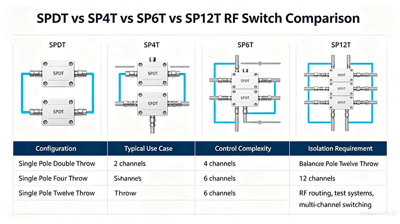
Multi-throw RF switches share one input (the common port) among N output ports. The most common configurations are SPDT (2 throws), SP3T (3 throws), SP4T (4 throws), SP6T (6 throws), SP8T (8 throws), and SP12T (12 throws). Each additional throw adds internal complexity, insertion loss, and cost, while giving the system designer more routing flexibility.
SPDT is the most common switch topology in the industry — it is the basic building block of nearly every signal-routing application. SP4T and SP6T are popular in antenna tuning, filter banks, and multi-band cellular front-ends. SP8T through SP12T switches are common in test equipment, multi-antenna systems (5G MIMO, satellite diversity), and large phased-array calibration networks.
Trade-offs as N Increases
Every additional throw typically adds 0.1 to 0.3 dB of insertion loss and degrades port-to-port isolation by 2 to 5 dB. A high-quality SP12T may have 2.5 dB of insertion loss and 40 dB of isolation, while a quality SPDT may have 0.4 dB loss and 70 dB of isolation. For applications where loss and isolation are critical, multiple SPDT switches cascaded in a tree can outperform a single high-throw switch.
| Topology | Typical Insertion Loss | Typical Isolation | Common Applications |
|---|---|---|---|
| SPST | 0.2–0.5 dB | 25–50 dB | TX/RX enable, bypass |
| SPDT | 0.3–0.6 dB | 50–70 dB | TX/RX switching, two-antenna selection |
| SP4T | 0.5–1.0 dB | 45–60 dB | Filter banks, band selection |
| SP6T | 0.7–1.5 dB | 40–55 dB | Antenna tuning, 5G front-end |
| SP8T | 0.9–2.0 dB | 38–50 dB | Test equipment, multi-band radios |
| SP12T | 1.2–2.5 dB | 35–45 dB | Phased arrays, ATE matrices |
Pin Diode RF Switch
The PIN diode is one of the oldest and most widely deployed semiconductor RF switch technologies. A PIN diode is a three-layer device (P-type, Intrinsic, I-type, N-type) whose RF impedance is controlled by a DC bias current. At zero or reverse bias, the intrinsic region is depleted and the diode presents high impedance (open circuit). At forward bias, the intrinsic region fills with carriers and the diode presents low impedance (short circuit).
PIN diode switches are favored for applications requiring high power handling, fast switching, and broadband operation. They can switch kilowatts of CW power at HF/VHF frequencies and handle hundreds of watts at L-band. The intrinsic region's slow carrier recombination limits the upper frequency of PIN diodes to roughly 3–6 GHz in practical switch designs, though specialty devices push beyond.
PIN Diode Switch Topologies
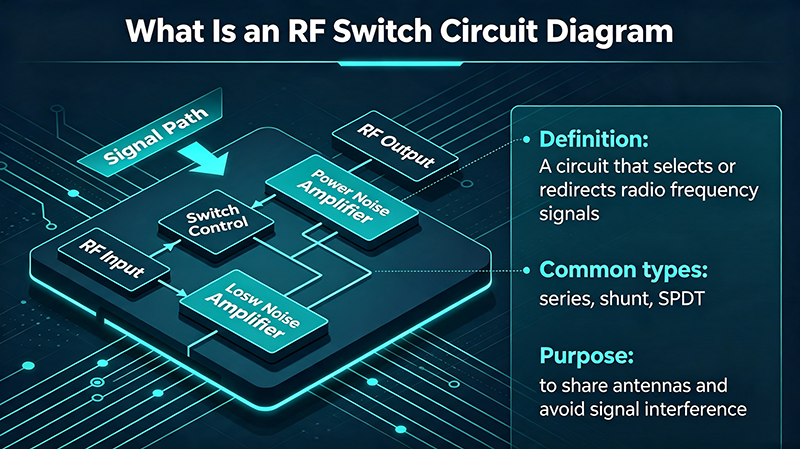
Two basic topologies dominate. The series PIN switch places a diode in series with the RF path; forward bias turns the switch on, reverse bias turns it off. The shunt PIN switch places a diode in shunt (across the line); forward bias shorts the line (switch off), reverse bias opens the line (switch on). Most high-performance PIN switches combine both: a series-shunt or shunt-series-shunt arrangement gives better isolation than a single diode.
Advantages and Limitations
Advantages: high power handling, broadband (octave or more), fast switching (nanoseconds to microseconds), low insertion loss at low frequencies. Limitations: requires DC bias current (5–100 mA), higher distortion at high power than GaAs switches, the intrinsic carrier storage limits high-frequency performance, and the bias network adds complexity to the PCB.
High Power RF Switches
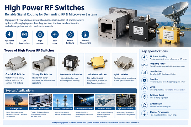
High-power RF switches are designed to handle transmit power levels from tens of watts up to multiple kilowatts. They are used in broadcast transmitters, radar systems, HF communications, and industrial heating equipment. The dominant technologies for high-power switching are electromechanical relays, PIN diode switches, and certain high-power MEMS designs.
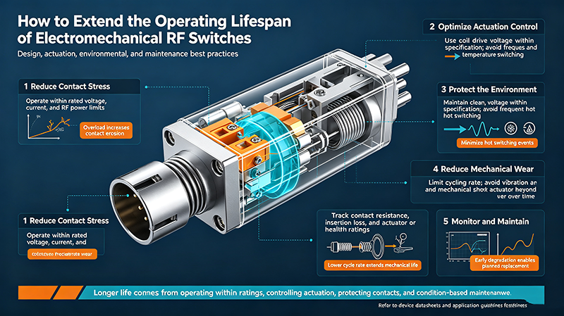
Electromechanical switches use a physical contact that moves to open or close the RF path. They offer the lowest loss and highest isolation of any switch technology, and can handle kilowatts of power at frequencies from DC to 67 GHz. The trade-off is slower switching speed (5–50 ms) and finite mechanical life (1–10 million cycles). Latching designs hold position without continuous current, ideal for solar-powered or battery-operated platforms.
Power Handling and Hot Switching
High-power switches are characterized by both peak power and average (CW) power ratings. Peak power handling is typically 2–10× the CW rating, because the thermal mass of the contact can absorb short transients. Hot-switching (switching while RF is present) derates the power handling — a switch rated for 100 W CW cold may only handle 10 W CW hot. For long switch life, always use cold switching in high-power applications.
| Switch Type | Max CW Power | Switching Speed | Best Use Case |
|---|---|---|---|
| Electromechanical (latching) | Up to 5 kW | 10–50 ms | Broadcast, radar, high-power TX |
| Electromechanical (non-latching) | Up to 2 kW | 5–25 ms | Fail-safe applications |
| PIN diode | Up to 1 kW (HF/VHF) | 1–10 µs | HF/VHF/UHF high-power |
| GaAs FET | Up to 10 W | 10–100 ns | Low-power fast switching |
| MEMS | Up to 5 W | 10–100 µs | Low-loss, high-isolation |
RF Switch Insertion Loss
Insertion loss is the amount of signal power absorbed or reflected by the switch when it is in the ON (passing) state. It is expressed in dB and is one of the most important specifications for any RF switch. A switch with 0.3 dB of insertion loss passes 93% of the input power; a switch with 1.0 dB passes 79%; a switch with 3.0 dB passes only 50%.
Insertion loss varies with frequency — it is lowest near DC and rises with frequency due to conductor loss, skin effect, and parasitic reactance. A switch with 0.3 dB of loss at 1 GHz might have 0.6 dB at 6 GHz and 1.2 dB at 18 GHz. Always check the insertion loss specification at your exact operating frequency, not at the headline number on the datasheet.
Why Insertion Loss Matters
Every 1 dB of switch loss in a receiver front-end raises the system noise figure by 1 dB (assuming the switch is before the LNA). Every 1 dB of switch loss in a transmitter reduces EIRP by 1 dB. In a 64-element phased array, the cumulative loss of the corporate feed network (which may contain 6 or 7 cascaded switches/dividers) can easily reach 6–10 dB, severely reducing the array's effective radiated power.
Reducing Effective Insertion Loss
Three strategies minimize the impact of switch insertion loss. First, place the switch as close to the source or load as possible — after the LNA in receive chains and before the PA in transmit chains. Second, choose a switch technology with low loss at your frequency (electromechanical at low frequencies, GaAs or MEMS at high frequencies). Third, consider a bypass switch that routes around a lossy stage when full performance is not needed.
RF Switch Isolation
Switch isolation is the amount of signal that leaks from the input to a port that should be isolated (typically the OFF port or a non-selected throw). It is measured in dB and is the second-most-critical specification after insertion loss. A switch with 60 dB of isolation leaks 0.0001% of the input power to the OFF port; a switch with 30 dB of isolation leaks 0.1% — 1000× more.
High isolation is essential in several applications. In transmit/receive (T/R) switching, high isolation prevents the transmit signal from leaking into the sensitive receive path, which could damage the LNA or desensitize the receiver. In local-oscillator distribution, high isolation prevents one channel's LO from appearing in another. In antenna selection, high isolation prevents cross-coupling between antennas.
How to Improve Isolation
Several design techniques improve isolation beyond the basic switch IC's specification. Adding a π-attenuator (3 dB pad on each side) at the switch's output improves isolation by 6 dB at the cost of 6 dB of additional loss. Using two switches in series doubles the isolation in dB. Adding a low-noise amplifier after the switch with high reverse isolation (S12 < −50 dB) further isolates the receive chain.
RF Switch VSWR
VSWR (Voltage Standing Wave Ratio) at a switch's ports indicates how well the switch is matched to the system impedance of 50 Ω (or 75 Ω in video/cable systems). A switch's input VSWR affects how much signal is reflected back toward the source; its output VSWR affects how the switch interacts with the downstream component. A typical quality RF switch has VSWR of 1.2:1 to 1.5:1 across its operating band.
VSWR becomes critical when switches are cascaded. Two switches each with 1.5:1 VSWR, when connected, can present a worst-case VSWR of 3:1 at the connection point because the reflections add. This is why matrix switches in production test systems are often specified with VSWR of 1.2:1 or better — to keep the cumulative VSWR within calibration accuracy.
Measuring Switch VSWR
Switch VSWR is measured with a vector network analyzer, with all unused ports terminated in 50 Ω loads. The ON path's input VSWR is measured by looking into the input while the switch is in the ON state. The OFF port's output VSWR is measured by looking into the output with the switch in the OFF state. Spec sheets typically distinguish "ON port VSWR" and "OFF port VSWR" because they can differ.
RF Switch Switching Speed
Switching speed is the time required for the switch to transition from one state to another. It ranges from nanoseconds (GaAs FET switches) to tens of milliseconds (electromechanical switches), spanning six orders of magnitude. The right speed depends on the application: radar beam steering needs microsecond switching, test equipment needs millisecond switching, and satellite payload redundancy needs second-scale switching.
Defining Switching Speed
Two specifications matter. The "switching time" is the time from the control signal change to the RF output reaching 90% (or 50%, depending on the manufacturer) of its final value. The "settling time" includes the additional time for the switch to stabilize within its specified insertion loss, isolation, and VSWR limits. Always specify the settling time, not just the switching time, in system timing budgets.
Speed vs Other Parameters
Switching speed trades against nearly every other parameter. Faster switches (GaAs) have higher insertion loss and lower power handling than slower switches (electromechanical). PIN diode switches are in between. MEMS switches offer electromechanical-class loss and isolation with microsecond switching, but at higher cost and lower power handling than electromechanical.
| Technology | Switching Time | Insertion Loss | Power Handling |
|---|---|---|---|
| GaAs FET | 10–100 ns | 0.5–1.5 dB @ 6 GHz | 0.1–10 W |
| PIN diode | 1–10 µs | 0.3–1.0 dB @ 2 GHz | 10–1000 W |
| MEMS | 10–100 µs | 0.1–0.5 dB @ 10 GHz | 1–5 W |
| Electromechanical | 5–50 ms | 0.05–0.3 dB @ 18 GHz | Up to 5 kW |
RF Switch Troubleshooting
When an RF switch misbehaves, the symptoms typically fall into four categories: high insertion loss, low isolation, high VSWR, or failure to switch. Each has a finite set of root causes, and a systematic approach identifies the problem in minutes rather than hours.
Common Failure Modes
High insertion loss: the most common cause in semiconductor switches is bias circuit failure — the control voltage is present but the bias current is not reaching the internal FET or PIN diode. Check the bias network with a multimeter and an oscilloscope. In electromechanical switches, the contact is worn or contaminated and needs replacement.
Low isolation: usually indicates a short or leakage path on the OFF port. In PIN diode switches, check the reverse bias voltage. In electromechanical switches, look for mechanical damage or contamination on the contact.
High VSWR: typically a connector problem (loose, damaged, or wrong torque) or a PCB trace issue. Reflow the connector or replace the cable first; only then suspect the switch.
Failure to switch: in semiconductor switches, check the logic levels on the control pins. In electromechanical switches, listen for the click — if you don't hear it, the coil is not being energized. Check the driver voltage and current.
Diagnostic Procedure
- Verify the control signal is present and at the correct logic level.
- Measure the switch's DC bias currents and compare to the datasheet.
- Measure S-parameters with a VNA, comparing ON-state and OFF-state traces against a known-good unit.
- Inspect connectors under magnification (200× minimum) for damage or contamination.
- Replace the switch with a known-good unit to isolate the failure to the switch vs the system.
RF Switch Matrix
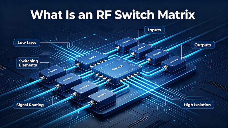
An RF switch matrix is a network of interconnected switches that allows any of M input ports to be connected to any of N output ports. Switch matrices are the workhorse of automated test equipment, large-scale antenna systems, and signal monitoring installations. They replace manual cable swapping with millisecond-speed electronic routing under software control.
Matrix Architectures
Three architectures dominate. The full crossbar (M×N switches, one at every crosspoint) provides maximum flexibility — any input can connect to any output — at the highest cost. The blocking matrix (M + N − 1 switches) provides limited flexibility at lower cost. The fan-out (one input to many outputs) is used in monitoring and broadcast applications. For most production ATE, full crossbar is the right answer despite its cost.
Critical Matrix Specifications
Insertion loss in a matrix is the sum of the through-path switch losses plus connector and cable losses. A 4×4 full crossbar with two switches per path has 0.5–1.5 dB of insertion loss; a 16×16 matrix with four switches per path has 1.5–3 dB. Isolation in a multi-stage matrix is the sum of the stages' isolations, minus 6 dB for the in-between mismatch — so a two-stage matrix with 60 dB per switch has roughly 108 dB total isolation, not 120 dB.
Crosspoint count is the size metric: a 32×32 matrix has 1024 crosspoints. Most modern matrices are software-controlled via USB, Ethernet, or LXI, with switching speeds of 10–50 ms per state change. For test systems requiring faster switching, look for solid-state matrix modules with nanosecond transitions.
RF Switch for 5G
5G New Radio (NR) imposes unique requirements on RF switches. The cellular bands span 600 MHz to 6 GHz in FR1 (sub-6 GHz) and 24–40 GHz in FR2 (mmWave). 5G phones must support 4G LTE, 5G NR, Wi-Fi, Bluetooth, and GNSS simultaneously, requiring dozens of switches in a small area. Carrier aggregation (combining multiple bands for higher data rates) requires switches that can isolate signals 80 dB or more between adjacent bands.
5G Switch Requirements
Key specifications for 5G handset switches: insertion loss below 0.5 dB at 3.5 GHz; isolation above 25 dB (preferably 30 dB); harmonic distortion below −70 dBc at +28 dBm input; switching speed below 5 µs for envelope tracking; power handling of at least 30 dBm for transmit paths; and CMOS control logic compatible with the handset's baseband. SOI (silicon-on-insulator) CMOS technology has become the dominant choice because it integrates the switch, bias network, and control logic on a single die at very low cost.
5G Base Station Switches
5G base stations have different requirements. They handle 4×4 or 8×8 MIMO with higher power (46 dBm typical), must operate across multiple bands in carrier aggregation, and require longer switching times (milliseconds are fine). PIN diode and GaAs switches are common in base stations because of their higher power handling, and the higher cost of base station equipment supports their higher unit price.
RF Switch for Radar
Radar systems use RF switches in transmit/receive (T/R) modules, beam-steering networks, and calibration paths. T/R switches in particular are mission-critical: they must isolate the sensitive LNA from the high-power PA during transmit, switch in microseconds to support pulsed radar, and handle kilowatts of peak power without breakdown.
T/R Switch Requirements
A T/R switch must provide at least 60 dB of isolation between the PA output and the LNA input during transmit. It must switch fast enough to support the radar's pulse repetition interval (often 1–10 µs for surveillance radar, sub-µs for fire-control radar). It must handle peak powers of 1–25 kW (for surveillance and fire-control radar) and 50–100 kW (for long-range early-warning radar). PIN diode and ferrite circulator-based T/R switches dominate this application.
Phased Array Radar
Modern phased array radars contain thousands of T/R modules, each with its own transmit/receive switch, phase shifter, and attenuator. The switch in each T/R module sees only a fraction of the total array power, but the cumulative cost of the switches dominates the array's bill of materials. GaAs and SiGe BiCMOS switches are common in modern X-band and Ku-band phased arrays because of their low cost, fast switching, and acceptable power handling.
RF Switch for Test Equipment
Test and measurement equipment — vector network analyzers, spectrum analyzers, signal generators, and production ATE — uses RF switches to route signals between instruments, calibration standards, and the device under test. The dominant switch technology in modern test equipment is electromechanical (for high isolation, low loss, and broadband) supplemented by solid-state (for fast switching).
VNA Internal Switches
A modern vector network analyzer contains 4–8 internal RF switches that route the source signal to the test ports, route the received signal to the receivers, and connect the calibration standards during calibration. These switches must have VSWR below 1.05:1 and insertion loss below 0.05 dB at the test ports to preserve the VNA's calibrated accuracy. The most demanding VNA designs use latching electromechanical switches because they hold position without continuous current draw and have essentially unlimited life.
ATE Matrix Switches
Production automated test equipment uses large switching matrices (often 8×8 or 16×16) to connect multiple DUTs to multiple instruments. The matrix must support fast cold-switching (position the switch before applying RF), provide repeatable performance over millions of cycles, and integrate with standard test executives (LabVIEW, Python, C). Electromechanical switches are the standard for production ATE because of their high isolation, low loss, and long life. Solid-state matrix modules are emerging for applications requiring sub-millisecond switching.
Switch Verification and Calibration
Every switch in a test system should be verified at the system level during daily calibration. The calibration procedure should measure the through-path insertion loss, the through-path VSWR, and the isolation to all unselected ports. A switch that has drifted by more than 0.1 dB in insertion loss or 5 dB in isolation should be replaced before further testing. Maintaining a switch-replacement log allows trending of switch life and prediction of when preventive maintenance is needed.
Frequently Asked Questions
Conclusion
RF switches are fundamental components that enable the sophisticated signal routing required in modern wireless systems. Understanding what RF switches are, how they work, and the different types available helps engineers select the right component for their specific applications.
From simple SPDT switches in mobile phones to complex matrix switches in test equipment, these versatile devices serve critical functions across the entire spectrum of wireless technologies. Whether you need fast switching for radar, high isolation for receivers, or high power handling for transmitters, there is an RF switch technology optimized for your requirements.
As wireless systems continue to evolve with 5G, mmWave, and emerging 6G technologies, RF switches will remain essential building blocks. Advances in semiconductor technology, MEMS, and integrated designs promise even better performance and integration in the years ahead.
Need Help Choosing the Right RF Switch?
Our technical team can help you understand RF switch options and select the optimal component for your specific application.
Contact Our Technical Team