






RF Switch Design in High-Frequency Communication Systems
Table of Contents
- 1. The Role of the RF Switch in Modern Systems
- 2. Design Challenges at High Frequency
- 3. Switch Topologies & Architectures
- 4. Semiconductor Technologies Compared
- 5. Critical Design Parameters
- 6. PCB Layout & Packaging
- 7. Thermal & Power Considerations
- 8. Application Examples
- 9. Design Workflow
- 10. Frequently Asked Questions
- 11. Conclusion
1. The Role of the RF Switch in Modern Systems
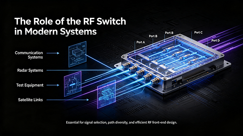
An RF switch routes high-frequency signals between multiple paths under electronic or electromechanical control. In modern high-frequency communication systems, switches perform several mission-critical functions:
- Antenna switching between multiple radiating elements (MIMO, beamforming).
- Transmit / Receive (T/R) duplexing in radios and radar front-ends.
- Band selection across multi-band transceivers (sub-6 GHz, mmWave, satellite).
- Redundancy routing for fail-safe aerospace and defense systems.
- Calibration path selection in ATE and production test.
- Phase-array reconfiguration in electronically steered antennas.
At mmWave frequencies, even a few tenths of a dB of insertion loss can erode link budget dramatically — making the RF switch one of the highest-leverage components in the signal chain.
2. Design Challenges at High Frequency
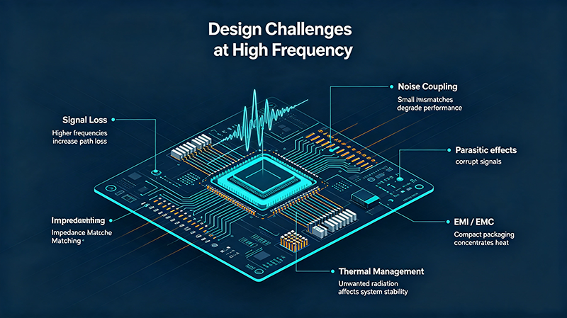
Designing RF switches for high-frequency communication systems introduces unique challenges:
- Insertion loss rises with frequency due to conductor and dielectric losses.
- Parasitic capacitance and inductance from packaging and bond wires become dominant.
- Isolation degrades as capacitive coupling paths leak more energy.
- VSWR worsens from any impedance discontinuity at the mmWave scale.
- Switching speed vs. isolation trade-off — faster devices often leak more.
- Power handling drops as semiconductor breakdown voltages shrink at smaller process nodes.
- Thermal density increases in compact mmWave modules.
3. Switch Topologies & Architectures
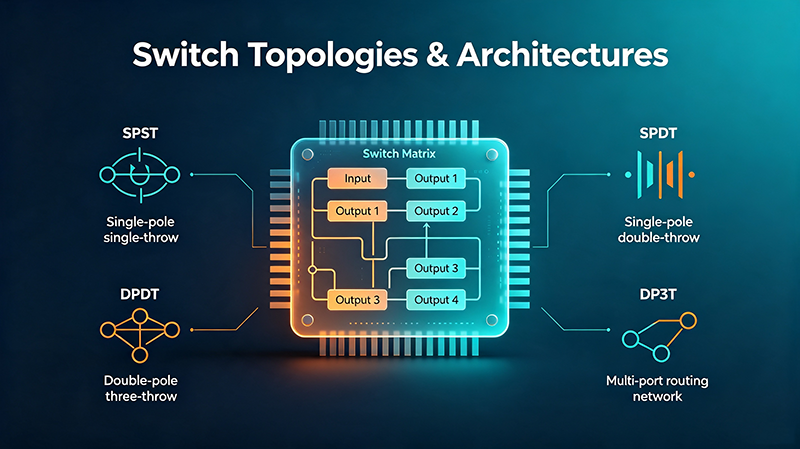
3.1 Series-Shunt Topology
The most common PIN-diode and FET switch architecture. Series devices block the OFF path; shunt devices short the OFF path to ground. Combining both improves isolation without sacrificing insertion loss.
3.2 Absorptive vs. Reflective
Reflective switches are simpler and lower loss, but reflect energy back when OFF. Absorptive switches terminate the OFF path with 50 Ω, ideal for sensitive filter networks and high-isolation applications.
3.3 SPDT / DPDT / SPnT
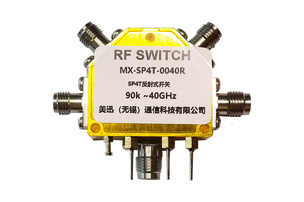
Switch count scales with port count. SPnT switches (SP4T, SP6T, SP12T) are widely used in 5G front-end modules and ATE matrices.
3.4 Differential / Balanced Switches
Used in differential signal chains to improve common-mode rejection and even-order distortion.
4. Semiconductor Technologies Compared
| Technology | Frequency | Insertion Loss | Switching Speed | Power Handling | Typical Use |
|---|---|---|---|---|---|
| PIN Diode (Si) | DC–18 GHz | 0.3–0.8 dB | 10–100 ns | High (> 10 W) | T/R switching, antenna tuning |
| GaAs FET | DC–40 GHz | 0.5–1.2 dB | < 10 ns | Medium (~ 1 W) | Test & measurement, broadband |
| SOI CMOS | DC–60 GHz | 0.7–1.5 dB | < 100 ns | Low (~ 0.5 W) | 5G, mmWave, mobile |
| SiGe HBT | DC–110 GHz | 1.0–2.0 dB | < 20 ns | Low | mmWave beamforming |
| RF MEMS | DC–80 GHz | 0.1–0.3 dB | µs | Medium | Low-loss test, instrumentation |
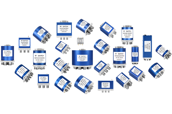
| Electromechanical (Relay) | DC–40 GHz | 0.2–0.4 dB | 10–25 ms | Very high | Coaxial lab switches, redundancy |
5. Critical Design Parameters
Insertion Loss (IL)
Signal loss in the ON state. Minimizing IL extends battery life and link range.
Isolation
Signal leakage to the OFF port. Critical for T/R switching and filter protection.
Return Loss / VSWR
Impedance match at each port. > 15 dB return loss is typical for mmWave designs.
P1dB / IP3
Linearity. The 1 dB compression point and third-order intercept define large-signal behavior.
Switching Speed
Rise/fall time and settling time. 5G beamforming requires < 1 µs switching.
Power Handling
Maximum CW and peak RF power before compression or damage.
DC Bias Current
Quiescent current draw. Critical for battery-powered mobile devices.
Phase Invariance
Phase shift between ON/OFF states. Must be stable for coherent beamforming.
6. PCB Layout & Packaging
At high frequencies, the PCB is part of the circuit. Follow these guidelines:
- Use controlled-impedance microstrip or stripline routing (50 Ω nominal).
- Keep ground vias dense and short to suppress parasitic inductance.
- Avoid right-angle bends — use mitered or curved traces to reduce reflections.
- Place DC blocking capacitors close to RF pins to isolate bias networks.
- Use short bond wires or flip-chip for the smallest possible parasitic loop.
- Shield RF traces with via fences to reduce coupling and radiation.
- Select low-loss laminates such as RO4350B, RO4003C, or PTFE for > 20 GHz designs.
7. Thermal & Power Considerations
High-frequency switches can dissipate significant heat, especially in T/R modules that toggle rapidly under high RF power.
- Use thermal vias beneath the die pad to conduct heat to internal ground planes.
- Select packaging with exposed paddle for direct PCB heatsinking.
- Avoid hot-switching — sequence control so RF power is off before switching.
- For PIN-diode switches, use a current-limiting resistor to prevent thermal runaway.
- Monitor junction temperature — derate performance above 85 °C ambient.
8. Application Examples
8.1 5G / mmWave Front-End
Phased-array antennas use thousands of switches to reconfigure beam direction in microseconds. SOI CMOS switches dominate due to integration and cost.
8.2 Satellite Communication
Ku-band and Ka-band satellite terminals require low-loss, high-isolation switches for uplink/downlink routing. GaAs and RF MEMS are common choices.
8.3 Radar Systems
Pulsed radar uses T/R switches to protect sensitive LNAs from high-power transmit pulses. PIN diodes are favored for their power handling and speed.
8.4 Test & Measurement
VNA and ATE systems use electromechanical and solid-state switches for ultra-low loss and long cycle life across decades of bandwidth.
9. Design Workflow
Specs
Frequency, IL, isolation, power, speed.
Topology
SPDT, SPnT, absorptive vs. reflective.
Technology
PIN, GaAs, SOI, MEMS, or relay.
Verify
Sim, prototype, VNA test, sign-off.
10. Frequently Asked Questions
Q1: Which RF switch technology is best for 28 GHz 5G?
SOI CMOS is the most widely used thanks to its integration density and acceptable loss. For lowest insertion loss, GaAs or RF MEMS are better but more expensive.
Q2: How do I choose between absorptive and reflective switches?
Use absorptive switches when the OFF port connects to a sensitive filter or amplifier. Use reflective switches for simpler, lower-loss paths where reflection is acceptable.
Q3: Can I hot-switch a PIN diode switch?
Yes, PIN diodes tolerate hot-switching better than FETs due to their stored-charge behavior. But continuous hot-switching still reduces lifetime and linearity.
Q4: What is the biggest loss contributor in mmWave switches?
At > 24 GHz, packaging parasitics and bond-wire inductance dominate. Flip-chip or wafer-level packages dramatically reduce loss.
Q5: How do I improve isolation in a high-frequency switch?
Use series-shunt topologies, add a λ/4 transmission line between stages, and consider stacked FET configurations for 50+ dB isolation.
Q6: Are RF switches linear?
Solid-state switches introduce harmonic and intermodulation distortion, especially near compression. For highest linearity, use PIN diodes with adequate bias current, or MEMS switches.
11. Conclusion
RF switch design in high-frequency communication systems is a multi-dimensional optimization of frequency, insertion loss, isolation, switching speed, power handling, and integration. By selecting the right topology, semiconductor technology, and PCB layout approach, and by following the structured design workflow outlined above, you can build switches that meet the demanding requirements of 5G, mmWave, satellite, and radar systems. As frequencies climb and integration tightens, RF switches will continue to be one of the most strategic components in any modern wireless front-end.
About the Author — MeiXun Team
Chief Engineer Wang
High-tech Enterprise, Feifeng Talent
Chief Engineer Wang graduated with a master's degree in high-power microwave from the Institute of Electronics, University of Chinese Academy of Sciences.
View Full Profile- RF Switch Circuit Diagram
- RF Switch
- Ohm's Law
- dBm to Watt
- mW to dBm
- Wavelength to Frequency
- RF Connector
- SMA Connector
- RF Switch Module
- RF Coupler
- RF PIN Switch
- Microwave Coaxial Switch
- PIN Switch
- Coaxial RF Switch
- Waveguide Switch
- Microwave Switch
- Low Noise Amplifier
- PIN Diode Switch
- Coaxial Switch
- RF Microwave Switch
- SPST Switch