






RF PIN Switch-Complete Professional Guide
Introduction to RF PIN Switches
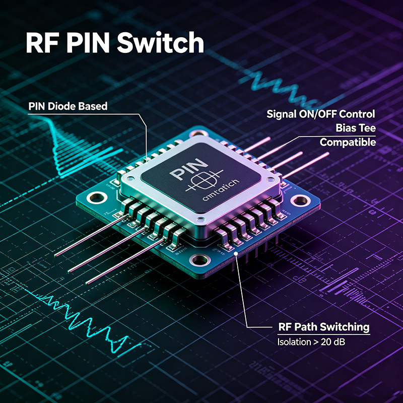
An RF PIN switch is a solid-state switching device that utilizes PIN diodes to control the flow of radio frequency signals in microwave and RF circuits. Unlike conventional PN junction diodes, the PIN diode features a wide intrinsic (I) region sandwiched between heavily doped P-type and N-type semiconductor layers. This unique structural characteristic gives the PIN diode its distinctive behavior at high frequencies: it behaves as a voltage-controlled variable resistor rather than a standard rectifying diode.
RF PIN switches are ubiquitous in modern wireless communication systems, radar equipment, test instrumentation, and satellite transceivers. They offer exceptional linearity, fast switching speeds, high isolation, and the ability to handle substantial RF power levels, making them indispensable components in RF front-end architectures where signal routing, antenna selection, and transmit/receive mode transitions are required.
Operating Principle of the PIN Diode
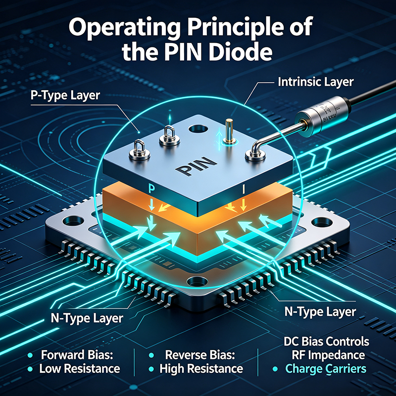
At DC and low frequencies, a PIN diode behaves much like a standard PN junction diode, conducting current when forward-biased and blocking current when reverse-biased. However, at RF and microwave frequencies, the behavior changes dramatically due to the charge storage properties of the intrinsic region. When the PIN diode is forward-biased with a DC current, the intrinsic region becomes flooded with charge carriers injected from the P and N regions. This stored charge creates a low-resistance conductive path that can pass RF signals with minimal attenuation, effectively placing the switch in its ON state.
When the PIN diode is reverse-biased or zero-biased, the intrinsic region becomes depleted of free charge carriers. Under these conditions, the diode presents a high impedance to RF signals, primarily capacitive in nature, which blocks signal transmission and places the switch in its OFF state. The transition between these two impedance states can occur extremely rapidly, typically within tens to hundreds of nanoseconds depending on the diode design and driver circuitry. The ratio between the OFF-state impedance and the ON-state impedance determines the isolation performance of the switch.
A critical requirement for proper PIN diode operation is that the RF signal frequency must be sufficiently high such that the period of the RF waveform is shorter than the carrier recombination time within the intrinsic region. This ensures that the diode does not rectify the RF signal and maintains its linear resistive behavior throughout each RF cycle, which is essential for minimizing signal distortion and harmonic generation.
Common RF PIN Switch Topologies
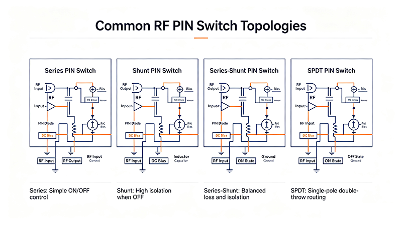
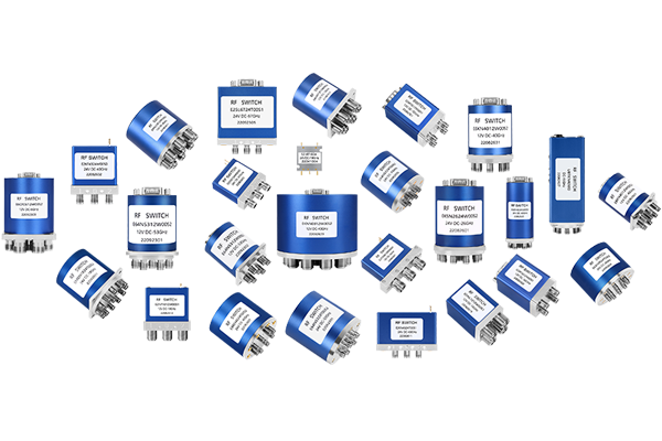
RF PIN switches are available in several standard configurations, each suited to specific system requirements. The most fundamental topology is the Single-Pole Single-Throw (SPST) switch, which functions as a simple on/off gate for an RF signal path. This basic building block can be implemented in either a series configuration, where the PIN diode is placed in line with the transmission path, or a shunt configuration, where the diode is placed between the transmission line and ground.
The Single-Pole Double-Throw (SPDT) switch is one of the most widely used configurations, capable of routing an input signal to one of two output ports. SPDT switches are commonly employed in antenna diversity systems and transmit/receive switching applications. More complex arrangements include Single-Pole Multi-Throw (SPnT) switches, which can route signals to three or more ports, and transfer switches (DPDT), which simultaneously connect two input ports to two output ports in either a straight-through or crossed configuration.
Series-shunt hybrid designs combine the advantages of both approaches, using series diodes to provide low insertion loss in the ON path while shunt diodes enhance isolation in the OFF paths. These multi-diode topologies achieve superior broadband performance and higher power handling compared to single-diode implementations, though they require more complex bias networks and consume additional DC power.
Key Performance Parameters
When selecting or designing an RF PIN switch, engineers must carefully evaluate several critical performance parameters that directly impact system-level functionality. Understanding these specifications is essential for matching the switch to its intended application and ensuring reliable operation across the required frequency range and environmental conditions.
Bias Networks and Driver Design
Proper biasing is fundamental to achieving optimal RF PIN switch performance. The bias network must supply the necessary forward current to each PIN diode in the ON state while maintaining a sufficient reverse voltage in the OFF state, all without interfering with the RF signal path. This is typically accomplished using bias tees, RF chokes, and DC blocking capacitors that separate the DC bias circuitry from the RF transmission lines.
The driver circuit controls the timing and amplitude of the bias signals applied to the PIN diodes. For high-speed applications, the driver must deliver rapid current transitions with minimal overshoot and ringing. Many modern PIN switch drivers incorporate shaping circuits that optimize the switching waveform to reduce video leakage and minimize switching transients that could interfere with sensitive receiver circuits or violate spectral emission requirements.
Thermal considerations also play a significant role in bias network design. As PIN diodes dissipate power during forward-biased operation, the resulting temperature rise can shift diode characteristics and affect long-term reliability. Adequate heat sinking, careful PCB layout with thermal vias, and conservative derating practices are essential for maintaining consistent switch performance over the full operating temperature range.
Comparison: PIN Switch vs. Alternative Technologies
| Parameter | PIN Diode Switch | GaAs FET Switch | MEMS Switch |
|---|---|---|---|
| Insertion Loss | Low to Moderate | Low | Very Low |
| Isolation | High (40-70 dB) | Moderate to High | High |
| Switching Speed | Fast (50-500 ns) | Very Fast (<50 ns) | Slow (1-100 μs) |
| Power Handling | High (Watts to kW) | Moderate | Low to Moderate |
| Linearity (IP3) | Excellent | Good | Excellent |
| DC Power Consumption | Moderate to High | Very Low | Near Zero |
| Lifetime / Reliability | Excellent | Excellent | Limited Cycles |
Applications Across Industries
RF PIN switches find widespread deployment across numerous industries due to their robust performance characteristics and design flexibility. In cellular base stations and small-cell infrastructure, PIN switches enable band selection, antenna beam steering, and transmit/receive switching in time-division duplex systems. Military and aerospace platforms rely on high-power PIN switches for radar pulse modulation, electronic warfare systems, and secure communication links where reliability under extreme conditions is paramount.
Test and measurement equipment, including vector network analyzers, spectrum analyzers, and signal generators, employ precision PIN switch matrices for automated signal routing and calibration path selection. Medical imaging systems such as MRI machines utilize specially designed PIN switches capable of handling the high peak powers and rapid switching sequences required for advanced imaging protocols. The burgeoning field of satellite communications, particularly in low-earth-orbit constellations, has driven demand for space-qualified PIN switches that combine low mass with exceptional radiation tolerance.
Design Challenges and Future Trends
Despite their maturity, RF PIN switch designs continue to face evolving challenges. The push toward higher frequencies in millimeter-wave 5G and 6G systems demands PIN diodes with ever-thinner intrinsic regions and reduced parasitic capacitances. Simultaneously, the trend toward smaller form factors in portable and wearable devices requires integrated switch solutions that combine multiple functions within single packaged modules. Thermal management at these high integration densities remains a persistent engineering challenge.
Emerging wide-bandgap semiconductor materials, including gallium nitride and silicon carbide, are being explored for PIN diode fabrication to achieve higher breakdown voltages and superior thermal conductivity. These advanced materials promise PIN switches capable of operating at higher temperatures and handling greater power densities than conventional silicon-based devices. Additionally, the integration of PIN switch cores with CMOS control logic and digital interfaces is enabling smart switches with built-in diagnostic capabilities, temperature compensation, and adaptive bias control that optimize performance dynamically based on operating conditions.
Looking forward, the convergence of RF PIN switch technology with advanced packaging techniques such as flip-chip assembly, wafer-level packaging, and heterogeneous integration will continue to push the boundaries of what is achievable in terms of size, cost, and performance. As wireless systems become increasingly complex and spectrum utilization intensifies, the RF PIN switch will remain a cornerstone component enabling the flexible, high-performance RF front-ends of tomorrow.
About the Author — MeiXun Team
Chief Engineer Wang
High-tech Enterprise, Feifeng Talent
Chief Engineer Wang graduated with a master's degree in high-power microwave from the Institute of Electronics, University of Chinese Academy of Sciences.
View Full Profile- RF Switch Circuit Diagram
- RF Switch
- Ohm's Law
- dBm to Watt
- mW to dBm
- Wavelength to Frequency
- RF Connector
- SMA Connector
- RF Switch Module
- RF Coupler
- RF PIN Switch
- Microwave Coaxial Switch
- PIN Switch
- Coaxial RF Switch
- Waveguide Switch
- Microwave Switch
- Low Noise Amplifier
- PIN Diode Switch
- Coaxial Switch
- RF Microwave Switch
- SPST Switch