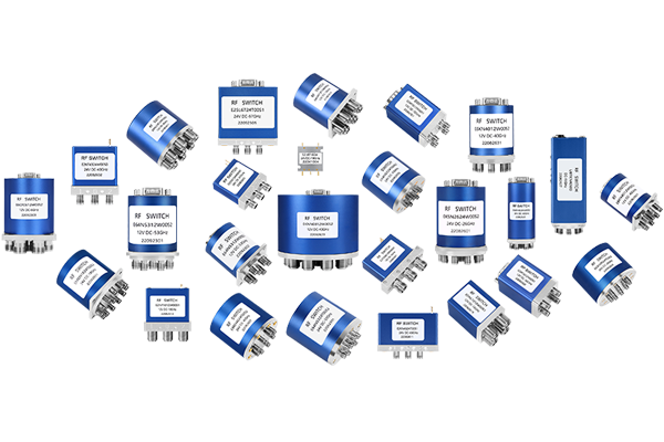
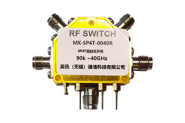
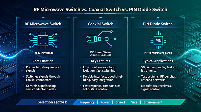
PIN diode switches are widely used in RF and microwave systems because of their
high switching speed, excellent isolation, low insertion loss, and ability to
handle high-frequency signals. They are commonly found in radar systems, wireless
communication equipment, test instruments, satellite systems, and electronic
warfare applications.
However, achieving optimal PIN diode switch performance requires careful design
considerations, including diode selection, bias network optimization, impedance
matching, thermal management, and PCB layout. This guide explains the key factors
that affect PIN diode switch performance and provides practical methods to improve
RF characteristics.
Understanding PIN Diode Switch Performance Parameters
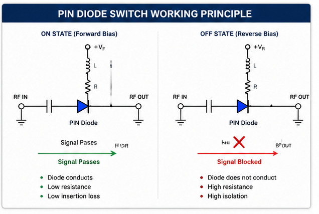
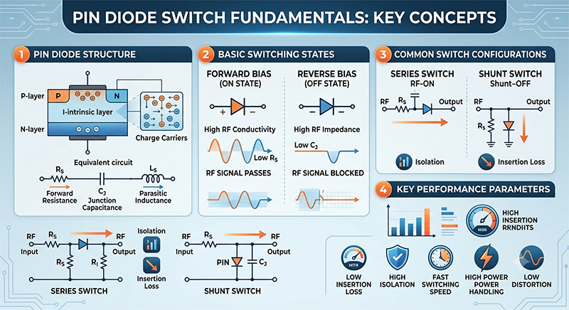
The performance of a PIN diode switch is determined by several critical RF parameters.
Improving these specifications can significantly enhance the overall system efficiency.
|
Parameter
|
Description
|
Optimization Goal
|
|
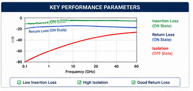
Insertion Loss
|
The signal loss when the switch is in the ON state.
|
Achieve the lowest possible loss.
|
|
Isolation
|
The ability to block unwanted signals in the OFF state.
|
Maximize signal separation.
|
|
Switching Speed
|
The time required to transition between ON and OFF states.
|
Reduce switching delay.
|
|
Power Handling
|
The maximum RF power the switch can handle.
|
Prevent diode damage and distortion.
|
|
Return Loss
|
Signal reflection caused by impedance mismatch.
|
Maintain good impedance matching.
|
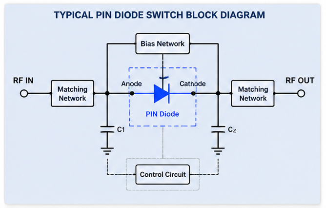
1. Select the Right PIN Diode for Your Application
Choosing the appropriate PIN diode is the first step toward improving switch
performance. Different applications require different diode characteristics.
Key Diode Parameters to Consider
-
Forward Resistance: Lower forward resistance reduces insertion loss
when the diode is conducting.
-
Reverse Resistance: Higher reverse resistance improves isolation
during the OFF state.
-
Carrier Lifetime: Determines switching speed and affects RF
performance at high frequencies.
-
Junction Capacitance: Lower capacitance improves isolation,
especially at microwave frequencies.
For high-frequency microwave switches, selecting PIN diodes with low parasitic
capacitance and optimized carrier lifetime is essential for achieving excellent
isolation and fast switching performance.
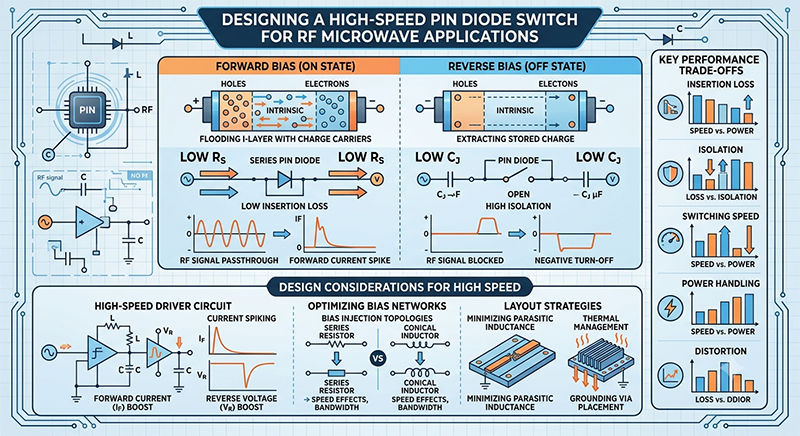
2. Optimize the Bias Circuit Design
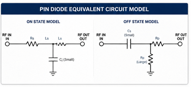
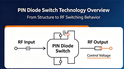
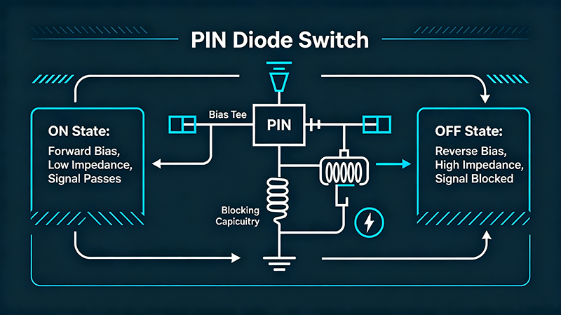
The bias network controls the operating state of the PIN diode. Poor bias design can
introduce additional losses, reduce isolation, and slow down switching response.
Methods to Improve Bias Performance
-
Use high-quality RF chokes to provide DC bias while blocking RF signals.
-
Add bypass capacitors to create a low-impedance RF ground path.
-
Ensure sufficient forward current to fully turn on the diode.
-
Avoid excessive bias current that increases power consumption and thermal stress.
3. Improve Impedance Matching
Impedance mismatch is one of the main causes of increased insertion loss and signal
reflection in PIN diode switches.
Maintaining a 50-ohm characteristic impedance throughout the RF path helps minimize
VSWR and improves signal transmission efficiency.
Common Matching Techniques
-
Microstrip impedance matching networks.
-
Quarter-wave transformer structures.
-
LC matching circuits.
-
RF simulation optimization using electromagnetic simulation tools.
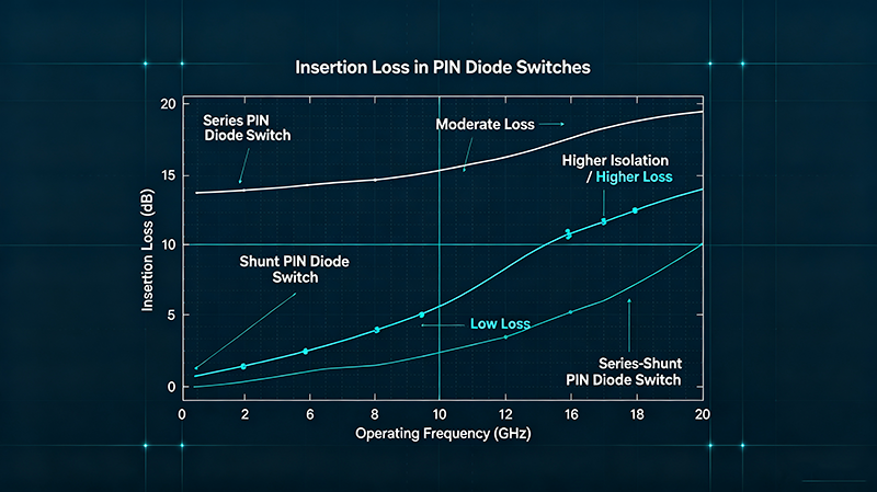
4. Reduce Insertion Loss
Low insertion loss is critical in RF applications because signal attenuation directly
affects system sensitivity and output power.
Ways to Reduce Insertion Loss
-
Select PIN diodes with low ON resistance.
-
Minimize PCB transmission line losses.
-
Reduce unnecessary RF connections and discontinuities.
-
Optimize the diode mounting structure.
5. Increase Switch Isolation
Isolation determines how effectively the switch prevents unwanted RF leakage when it
is turned OFF. High isolation is especially important in radar and communication
systems.
Techniques for Better Isolation
-
Use PIN diodes with lower junction capacitance.
-
Improve RF grounding design.
-
Optimize transmission line spacing.
-
Add additional isolation structures when required.
6. Optimize PCB Layout Design
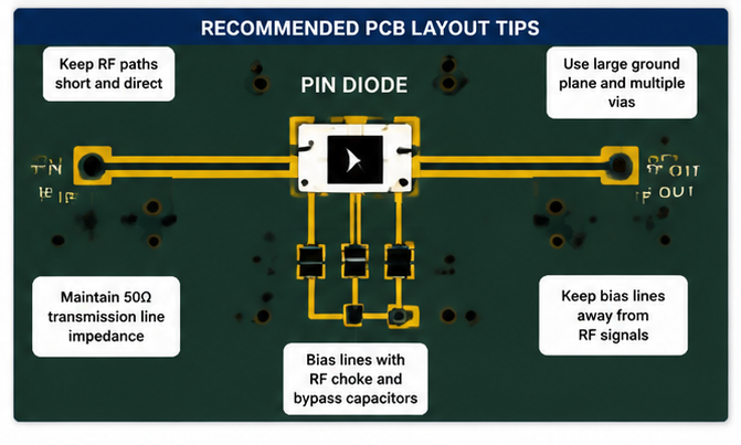
PCB layout has a significant impact on PIN diode switch performance, especially at
microwave frequencies.
-
Keep RF signal paths short and direct.
-
Maintain consistent transmission line impedance.
-
Use proper grounding techniques with multiple vias.
-
Separate RF paths from digital control signals.
-
Avoid sharp corners in high-frequency transmission lines.
7. Manage Thermal Effects
Temperature variations can affect PIN diode characteristics, including resistance,
switching speed, and reliability.
Proper thermal management improves long-term stability and prevents performance
degradation in high-power RF applications.
Thermal Optimization Methods
-
Use proper heat dissipation structures.
-
Select components rated for the operating temperature range.
-
Avoid excessive forward current.
-
Perform thermal simulation during design.
8. Use RF Simulation and Testing
Advanced simulation and measurement techniques help identify performance issues
before production.
Recommended Tools and Measurements
-
Vector Network Analyzer (VNA) for insertion loss and isolation testing.
-
Electromagnetic simulation software for RF optimization.
-
Time-domain measurements for switching analysis.
-
Thermal testing for high-power applications.
Common PIN Diode Switch Performance Problems
|
Problem
|
Possible Cause
|
Solution
|
|
High Insertion Loss
|
High diode resistance or poor matching.
|
Select better diode and optimize RF design.
|
|
Low Isolation
|
High junction capacitance or poor grounding.
|
Improve diode selection and PCB layout.
|
|
Slow Switching
|
Incorrect bias control.
|
Optimize driver circuit and bias timing.
|
|
Signal Distortion
|
Excessive RF power or thermal issues.
|
Improve power handling design.
|
Applications Requiring High-Performance PIN Diode Switches

-
5G and wireless communication systems.
-
Radar and defense electronics.
-
Satellite communication equipment.
-
RF test and measurement instruments.
-
Microwave signal routing systems.
-
Electronic warfare systems.
Conclusion
Improving PIN diode switch performance requires a complete optimization approach
covering diode selection, bias circuit design, impedance matching, PCB layout,
thermal management, and RF testing.
By minimizing insertion loss, maximizing isolation, improving switching speed, and
maintaining reliable operation under different conditions, engineers can achieve
high-performance PIN diode switches suitable for advanced RF and microwave systems.