

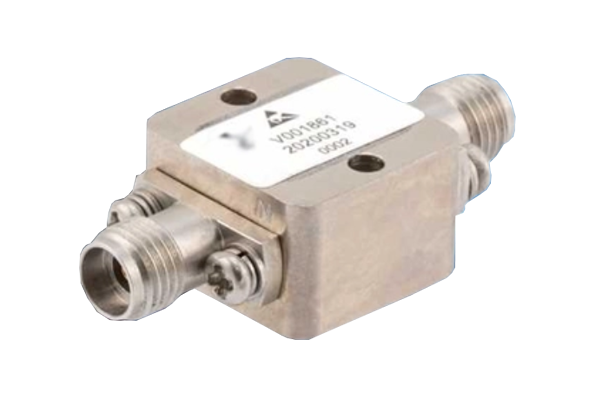
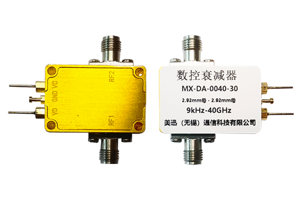
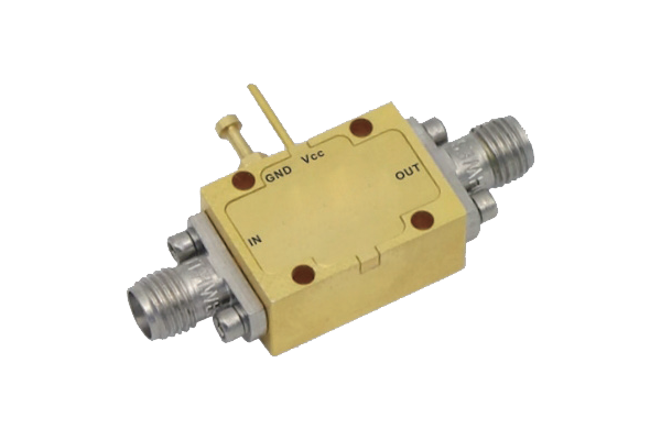
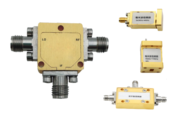




In high-frequency RF and microwave systems, controlling signal routing with high speed, low insertion loss, and excellent isolation is critical. While solid-state options like FETs are widely used, the PIN diode remains the gold standard for high-power, low-distortion RF switching applications. This comprehensive guide breaks down the core physics, equivalent circuit models, biasing configurations, and RF performance parameters of PIN diode switches to help you optimize your next RF design.
1. What is a PIN Diode? Core Physics and Operation
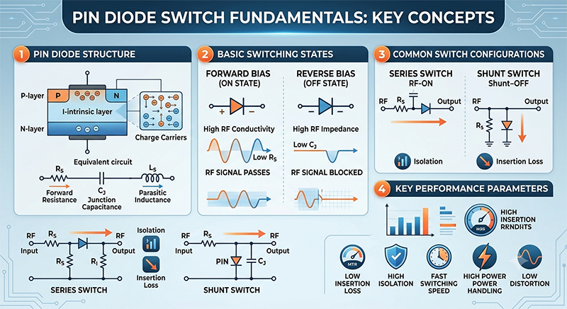
Unlike a standard PN junction diode, a PIN diode features a wide, undoped Intrinsic (I) layer sandwiched between highly doped P-type and N-type semiconductor regions. This unique physical structure determines its distinctive behavior at radio frequencies.
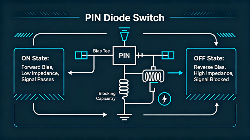
Forward Bias Operation (ON State)
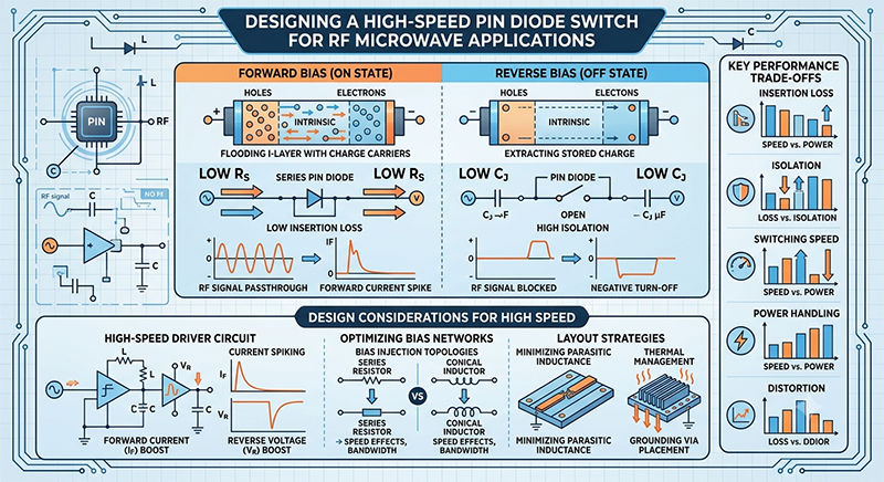
Under forward bias, holes and electrons are injected into the I-layer from the P and N regions. Because these carriers cannot recombine instantly, they create a stored charge that floods the intrinsic region. This drastically lowers its RF resistance to a fraction of an ohm (Rs), typically between 0.5 and 3 ohms depending on the diode design and forward current.
Rs = Rs0 * (I_F / I_F0)^-n where n typically 0.5-0.7
Reverse Bias Operation (OFF State)
Under zero or reverse bias, the I-layer is completely depleted of free carriers. The diode behaves primarily as a fixed, low-value capacitor (Cj), typically 0.1 to 1.0 pF, offering high impedance to RF signals.
Cj = ε * A / W where W is depletion width
Key Physical Properties
- Intrinsic Layer Width: Determines voltage handling and frequency response
- Carrier Lifetime (τ): Controls switching speed and distortion performance
- I-Layer Thickness: Trades off between power handling and speed
- Series Resistance: Lower Rs means lower insertion loss
- Junction Capacitance: Lower Cj means better high-frequency isolation
2. Equivalent Circuit Models
To design an effective RF switch, you must understand how the PIN diode presents itself to the RF signal in both states. The following equivalent circuits are used for circuit simulation and design.
| Parameter/State | Forward Bias (ON State) | Reverse Bias (OFF State) |
|---|---|---|
| RF Behavior | Low resistance (Rs) | Low capacitance (Cj) + High parallel resistance (Rp) |
| Typical Values | 0.5 Ω to 3 Ω | 0.1 pF to 1.0 pF |
| Circuit Equivalent | Series resistance (Rs) and parasitic inductance (Ls) | Parallel combination of Cj and Rp in series with Ls |
| Impedance Level | Very low (<< 50 Ω) | Very high (>> 50 Ω) |
| Frequency Response | Mostly flat to high frequency | Decreases with frequency (1/f) |
Component Descriptions
- Rs (Series Resistance): Forward-bias resistance, typically 0.5-3 Ω
- Cj (Junction Capacitance): Reverse-bias capacitance, typically 0.1-1.0 pF
- Rp (Parallel Resistance): High-value resistance (kΩ range) in reverse bias
- Ls (Parasitic Inductance): Package and bond wire inductance, typically 0.1-2 nH
3. Basic RF Switch Configurations
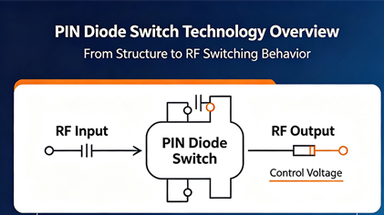
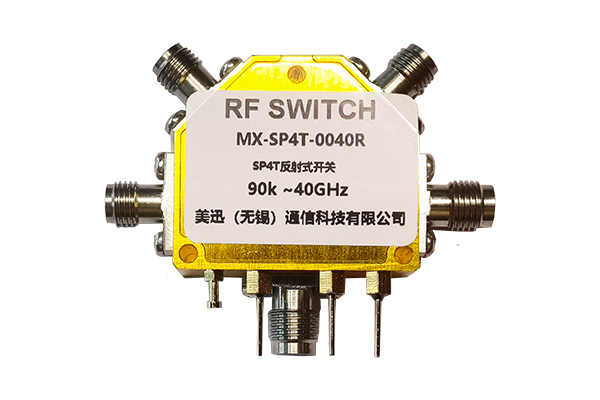
PIN diodes can be integrated into transmission lines in either Series or Shunt topologies to form Single-Pole Single-Throw (SPST) switches. These basic configurations can be combined to create more complex switch types like SPDT, SP4T, and matrix switches.
3A. Series Switch Configuration
In a series configuration, the diode is placed directly in line with the signal path, in series between input and output ports.
ON State (Forward Biased)
- Low resistance Rs allows signal to pass
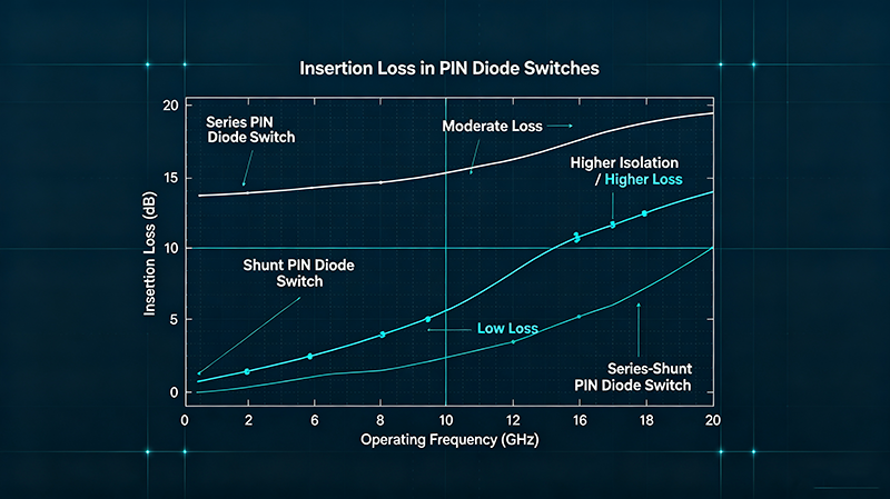
- Insertion loss typically 0.3-0.8 dB
- Minimal signal distortion
- Simple bias circuit
OFF State (Reverse Biased)
- Capacitive reactance of Cj blocks signal
- Isolation degrades at higher frequencies
- Capacitive coupling bypasses the open gap
- Limited to lower frequency applications
3B. Shunt Switch Configuration
In a shunt configuration, the diode is connected between the transmission line and the RF ground. This topology provides better high-frequency performance.
ON State (Reverse Biased)
- Diode acts as high-impedance path
- RF signal travels unimpeded
- Low insertion loss (0.2-0.5 dB)
- Excellent for high frequencies
OFF State (Forward Biased)
- Low resistance Rs creates near-perfect short to ground
- Reflects RF power back to source
- Provides high isolation (40+ dB)
- Requires careful bias network design
Isolation (dB) = 20*log10(1 + Z0/(2*Rs)) for Z0 = 50 Ω
Why Shunt Works Better at High Frequency
At high frequencies, the small capacitance Cj of the reverse-biased diode becomes a low impedance path to ground. This effectively shunts RF signals to ground, providing excellent isolation. The quarter-wave transformer effect makes this topology particularly effective at microwave frequencies.
4. DC Biasing Networks: The Key to Isolating RF from DC
A major challenge in PIN diode switch design is applying the DC control voltages without degrading or leaking the RF signal. This requires a robust bias network containing several critical components:
Essential Bias Network Components
RF Chokes (RFC)
Large inductors that block high-frequency RF signals while presenting zero resistance to DC currents. They allow DC bias to reach the diode while preventing RF from leaking into the DC supply lines.
- Typical values: 10-1000 nH depending on frequency
- Self-resonant frequency must exceed operating frequency
- Use chip inductors for best RF performance
DC Blocking Capacitors
Capacitors placed in series with the RF path to prevent DC control currents from flowing back into the RF source or load. They pass RF signals while blocking DC.
- Typical values: 10-100 pF for microwave frequencies
- Must have low ESR and ESL
- Use NP0/C0G ceramic or thin-film capacitors
Quarter-Wave (λ/4) Microstrip Lines
Often used at microwave frequencies instead of lumped inductors to act as open circuits at the design frequency. A quarter-wavelength line transforms a short circuit to an open circuit.
- Provides high impedance over wide bandwidth
- No parasitic resonances like lumped inductors
- More compact than equivalent lumped networks
Bias Network Design Tips
- Use multi-stage filtering for broadband isolation (10 pF + 100 pF + 10 nF + 1 µF)
- Place smallest capacitors closest to the diode
- Add ferrite beads for additional RF isolation at lower frequencies
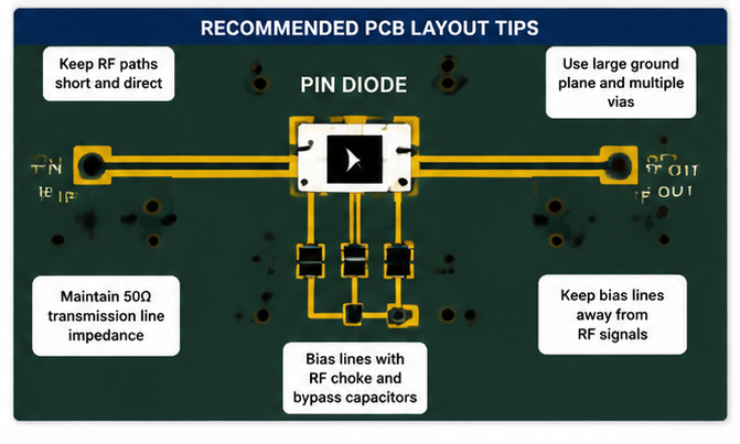
- Keep bias trace lengths short to minimize parasitic inductance
- Use separate bias feeds for each diode to prevent coupling
- Implement current limiting resistors to protect diodes
5. Key RF Performance Parameters
When selecting or designing a PIN diode switch, engineers must evaluate several overlapping trade-offs that directly impact system performance.
Primary Performance Parameters
Insertion Loss (dB)
The attenuation of the signal through the switch in its ON state. Lower series resistance (Rs) directly translates to lower insertion loss. Typical values range from 0.2-1.5 dB depending on frequency and configuration.
IL (dB) = 10*log10(1 + Rs/Z0) for Z0 = 50 Ω
Isolation (dB)
The attenuation through the switch in its OFF state. Minimizing junction capacitance (Cj) is critical for high isolation. PIN diode switches typically achieve 30-60 dB isolation across their operating frequency range.
Switching Speed
The time required to transition between ON and OFF states. This is dictated by the carrier lifetime (τ) of the intrinsic region and the speed of the driver circuit. Typical values range from nanoseconds to microseconds.
t_switch ≈ τ * ln(I_F/I_R) where τ is carrier lifetime
Power Handling
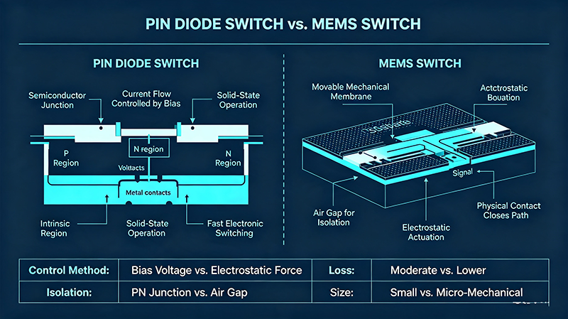
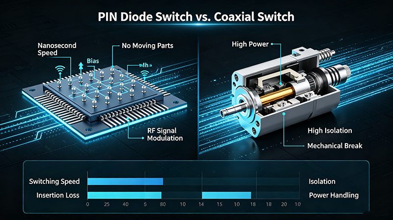
PIN diodes can handle high RF power because the thick I-layer distributes high voltage fields and withstands thermal heating better than GaAs or SOI FET switches. Power handling ranges from watts to hundreds of watts depending on design.
Linearity
PIN diodes exhibit excellent linearity due to their thick intrinsic region, which reduces nonlinear capacitance effects. This makes them ideal for high-order modulation systems like 256-QAM and 1024-QAM.
Frequency Range
PIN diode switches operate from VHF through millimeter-wave frequencies. Performance degrades at higher frequencies due to package parasitics and increased losses, requiring careful design for mmWave applications.
| Parameter | Typical Range | Key Trade-off |
|---|---|---|
| Insertion Loss | 0.2 - 1.5 dB | Frequency vs diode Rs |
| Isolation | 30 - 60 dB | Cj vs switching speed |
| Switching Speed | 1 ns - 10 µs | Speed vs power handling |
| Power Handling | 0.1 - 100 W | Power vs speed vs frequency |
| Frequency Range | 100 MHz - 50 GHz | Frequency vs insertion loss |
6. PIN Diode Switch Design Best Practices
Implementing a successful PIN diode switch design requires attention to multiple factors throughout the design process. These best practices help optimize performance and avoid common pitfalls.
Design Process Recommendations
- Start with specifications: Define frequency, power, speed, and isolation requirements clearly
- Choose topology: Series for simplicity, shunt for high frequency, series-shunt for best performance
- Select diodes: Match Rs and Cj to your frequency and performance requirements
- Design matching networks: Account for diode impedance variations between states
- Implement bias networks: Use proper RF chokes and DC blocking capacitors
- Optimize layout: Minimize parasitic inductance and maintain ground integrity
- Verify with simulation: Use harmonic balance and EM simulation for accuracy
- Test thoroughly: Measure all parameters across frequency and temperature ranges
Common Design Mistakes to Avoid
Advanced Design Techniques
- Series-Shunt Configuration: Combines advantages of both topologies for optimal performance
- Bridge Configuration: Four diodes in bridge arrangement for balanced switching
- Compensated Matching: Network design that accounts for diode impedance variations
- Thermal Compensation: Bias circuits that maintain performance across temperature
- Integrated Modules: Pre-built switch modules reduce design time and risk
Frequently Asked Questions
Conclusion
Mastering the design of PIN diode switches requires balancing physical limitations—such as carrier lifetime and junction capacitance—against layout practicalities like DC bias isolation. By carefully choosing between series and shunt configurations and implementing high-Q biasing elements, you can design high-performance, robust RF switches for telecommunications, radar, and test equipment applications.
Understanding the fundamental physics, equivalent circuit models, and key performance parameters enables engineers to make informed decisions about PIN diode selection, topology choice, and bias network design. The result is a switch that delivers optimal performance for your specific application requirements.
PIN diode switches continue to be a cornerstone technology in RF and microwave engineering, offering a unique combination of high power handling, excellent linearity, and proven reliability that keeps them relevant in modern wireless systems alongside newer semiconductor technologies.
Need Help with PIN Diode Switch Design?
Our engineering team can help you select the right PIN diodes and design optimal switching circuits for your specific RF application requirements.
Contact Our Technical Team