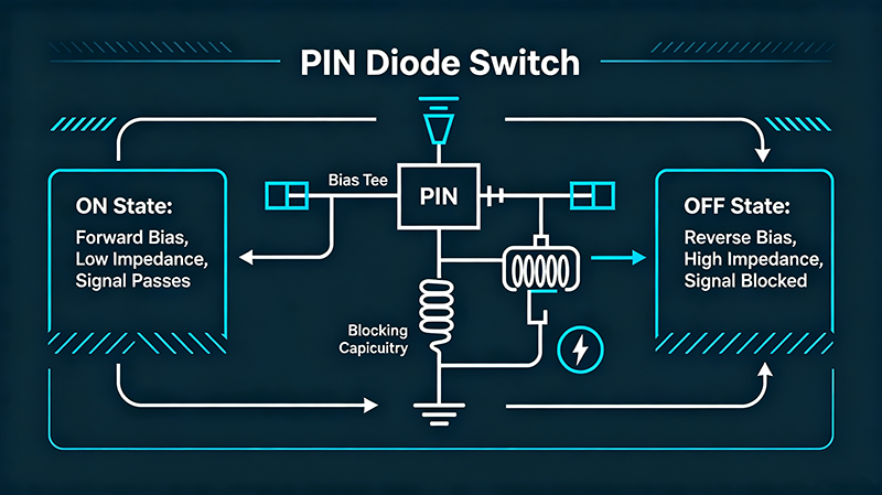


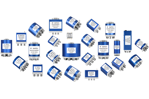
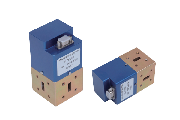
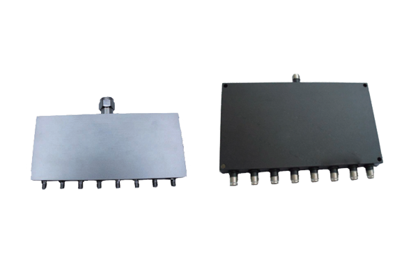




Insertion loss is one of the most critical performance parameters in PIN diode switch design. Every decibel of loss directly impacts system sensitivity, reduces signal power, and degrades overall RF performance. This comprehensive guide provides practical, actionable techniques to minimize insertion loss in your PIN diode switch designs.
Understanding Insertion Loss in PIN Diode Switches
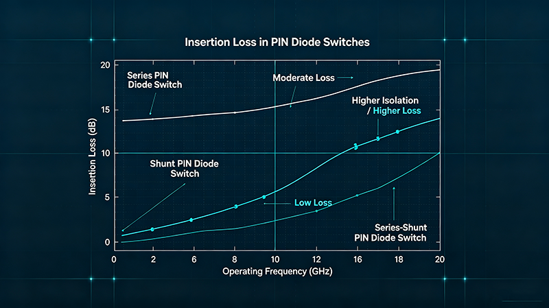
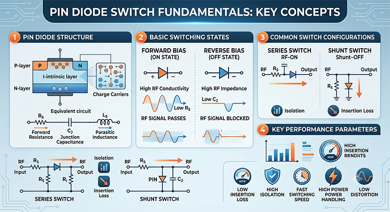
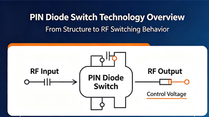
Insertion loss in PIN diode switches results from several factors, including the intrinsic resistance of the forward-biased diode, junction capacitance in the reverse-biased state, parasitic inductance from leads and packaging, and losses in matching components and transmission lines.
IL_total = IL_resistive + IL_matching + IL_transition + IL_substrate
Key Sources of Insertion Loss
| Loss Source | Typical Contribution | Mitigation Strategy |
|---|---|---|
| Diode Forward Resistance (Rs) | 0.3 - 1.0 dB | Select low Rs diodes, optimize bias current |
| Junction Capacitance (Cj) | 0.1 - 0.5 dB | Use high-resistivity substrate, proper biasing |
| Matching Network Losses | 0.1 - 0.3 dB | Use quality components, optimize design |
| Transition/Connector Losses | 0.05 - 0.2 dB | Quality connectors, proper assembly |
| Substrate Microstrip Losses | 0.05 - 0.15 dB | Use low-loss substrates, optimal line width |
Optimize PIN Diode Selection
Selecting the right PIN diode is fundamental to achieving low insertion loss. The diode's intrinsic resistance, junction capacitance, and carrier lifetime must be optimized for your specific frequency and application requirements.
Key Diode Parameters for Low Loss
Target Specifications
- Low Series Resistance (Rs): Target Rs < 2 ohms for frequencies below 10 GHz
- Low Junction Capacitance (Cj): Target Cj < 1 pF for microwave frequencies
- Fast Carrier Lifetime: Balances switching speed with low loss
- High I-region Thickness: Better isolation but higher Rs trade-off
- Low Thermal Resistance: Maintains performance under bias heating
Diode Technology Comparison
| Technology | Typical Rs | Typical Cj | Best For |
|---|---|---|---|
| GaAs Beam Lead | 1-3 ohms | 0.1-0.3 pF | mmWave, low loss |
| Silicon Planar | 1-5 ohms | 0.5-2 pF | Low frequency, cost |
| InP PIN | 0.5-2 ohms | 0.05-0.2 pF | Extremely low loss |
Optimize Circuit Topology
The switch circuit topology significantly impacts insertion loss. Different configurations offer different trade-offs between insertion loss, isolation, and complexity.
Common Switch Topologies
Avoid: Basic Series Only
- Simple but limited isolation
- Requires high-quality diodes
- Limited frequency range
- Higher VSWR
Prefer: Series-Shunt Configuration
- Improved isolation
- Better impedance matching
- Reduced VSWR
- More design flexibility
Bridge Configuration Benefits
For applications requiring the lowest insertion loss, consider the bridge topology:
- Four diodes in bridge arrangement
- Signal passes through two diodes in series when on
- Better balance and symmetry
- Improved common-mode rejection
- Typical loss penalty: 0.2-0.5 dB vs. single diode
IL ~ 10*log10(1 + Rs/2/Z0) + losses from shunt path
Design Tip: Parallel Diodes
For very low loss requirements, consider paralleling multiple small-area PIN diodes. Each diode carries a portion of the current, reducing the effective series resistance. However, ensure symmetric layout to avoid imbalance.
Minimize Parasitic Effects
Parasitic inductance and capacitance can significantly increase insertion loss, especially at higher frequencies. Understanding and minimizing these parasitics is essential for optimal performance.
Parasitic Sources and Solutions
Parasitic Minimization Checklist
- Bond Wire Inductance: Use multiple short bond wires in parallel (0.5-1 nH per wire)
- Lead Inductance: Minimize lead length, use chip-scale packages
- Package Parasitics: Prefer chip-scale or no-package (bare die) options
- Via Inductance: Use multiple small vias, avoid long via stubs
- Pad Capacitance: Minimize pad size, use appropriate dielectric
Package Impact on Performance
| Package Type | Series L | Shunt C | IL Impact |
|---|---|---|---|
| Bare Die | < 0.1 nH | Minimal | Best |
| Beam Lead | 0.1-0.3 nH | Very low | Excellent |
| SOT-23 | 1-2 nH | 0.2-0.5 pF | Moderate |
| TO-39 | 2-4 nH | 0.5-1 pF | Limited to <3 GHz |
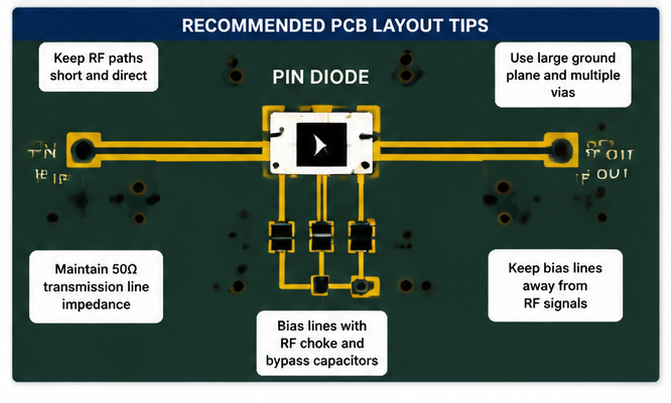
Optimize PCB Layout
PCB layout has a profound impact on PIN diode switch performance. Even with perfect component selection, poor layout can add significant insertion loss and degrade other parameters.
Layout Best Practices
Poor Layout Causes
- Long transmission lines
- 90-degree corners (use 45-degree)
- Thin ground plane
- Via stubs in signal path
- Inconsistent line width
- Ground slots near signal lines
Optimal Layout Techniques
- Shortest possible signal paths
- Mitered corners or smooth curves
- Continuous solid ground plane
- Blind/buried vias or no vias in RF path
- Controlled impedance lines
- Ground plane keepouts around sensitive areas
Substrate Selection
| Material | Dielectric Loss | Cost | Recommendation |
|---|---|---|---|
| Roger RT/duroid 5880 | Very low (0.0009) | High | Best performance |
| Rogers RO4003C | Low (0.0027) | Medium | Good balance |
| FR-4 | Moderate (0.02) | Low | < 3 GHz only |
IL_microstrip (dB/inch) = 8.68 * alpha_c + 8.68 * alpha_d
Grounding Strategy
Use via fencing around critical signal lines and place ground vias within 1mm of all ground connections. Ensure the ground plane beneath the PIN diode and matching network is solid and continuous.
Improve Impedance Matching
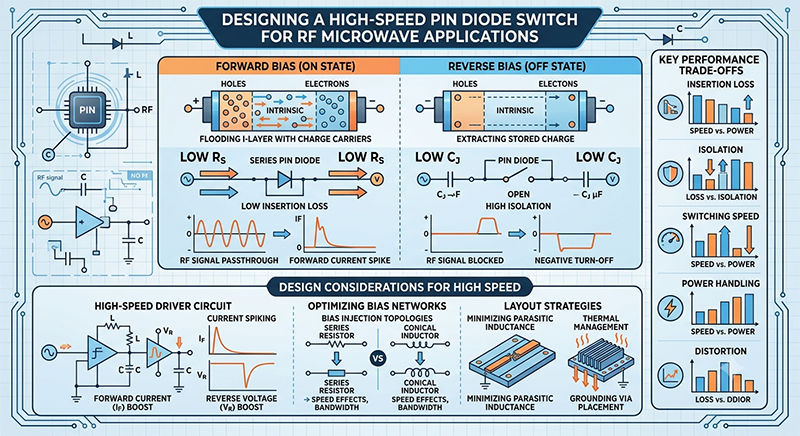
Proper impedance matching is essential for minimizing reflection losses and achieving optimal insertion loss. The PIN diode's impedance varies significantly between forward and reverse bias states.
Matching Considerations by State
Forward-Biased State (Low Loss Path)
- Target: Match diode Rs to system impedance (50 ohms)
- Use low-inductance matching elements
- Minimize matching network component count
- Consider transmission line transformers for broadband
Reverse-Biased State (High Isolation Path)
- Maximize impedance to present open circuit
- Account for junction capacitance resonance
- Use shunt configuration for better blocking
- Consider resonant stub techniques for high isolation
Matching Component Quality
| Component | Low Loss Option | Loss at 10 GHz |
|---|---|---|
| Capacitors | NP0/C0G ceramic, thin film | 0.02-0.05 dB |
| Inductors | Wire-wound, air core | 0.1-0.3 dB |
| Transmission Lines | Short, wide microstrip | Varies with substrate |
Optimize Bias Circuit Design
The bias circuit directly affects PIN diode performance in both states. Proper bias design ensures optimal forward resistance while maintaining high isolation in the reverse state.
Forward Bias Optimization
Forward bias current directly controls the diode's series resistance:
Rs = Rs0 * (I_F / I_F0)^-n where n typically 0.5-0.7
Bias Current Guidelines
- Minimum Current: Ensure sufficient current for low Rs (typically 1-10 mA)
- Current Density: Maintain adequate mA/um of diode area
- Thermal Limit: Avoid exceeding maximum current due to heating
- Saturation Point: Beyond certain current, additional gain is minimal
Bias Feed Network Design
Avoid in Bias Network
- Lumped inductors in series with RF path
- Long bias trace routing
- Poor RF bypassing
- Shared bias for multiple diodes
Preferred Bias Techniques
- Quarter-wave chokes at high frequencies
- Distributed bias line with adequate width
- Multi-stage decoupling (pF + nF + uF)
- Isolated bias networks per diode
Measuring and Verifying Insertion Loss
Accurate measurement of insertion loss is essential to verify your design optimizations. Use proper calibration and measurement techniques to avoid common errors.
Measurement Best Practices
- Use VNA Calibration: Perform full two-port SOLT calibration before measurement
- Reference Planes: Define reference planes at the device leads, not connectors
- Connector Quality: Use high-quality connectors and verify their condition
- Temperature: Measure at operating temperature as loss varies with temperature
- Averaging: Use appropriate averaging to reduce noise while maintaining speed
- Multiple Samples: Measure several units to account for manufacturing variation
IL (dB) = -10*log10(|S21|^2) including fixture losses
Frequently Asked Questions
Conclusion
Reducing insertion loss in PIN diode switches requires attention to multiple design factors. By carefully selecting diodes with appropriate Rs and Cj specifications, optimizing circuit topology, minimizing parasitic effects, implementing proper PCB layout, achieving excellent impedance matching, and designing robust bias circuits, you can achieve insertion loss close to the theoretical minimum.
Remember that insertion loss optimization must be balanced against other requirements including isolation, switching speed, power handling, and cost. Use EM simulation tools to verify your designs before fabrication, and always measure prototype performance to validate simulations.
The techniques outlined in this guide provide a systematic approach to minimizing insertion loss. Start with the fundamentals—diode selection and topology—then refine your design through layout optimization and matching improvements.
Need Help Optimizing Your PIN Diode Switch Design?
Our engineering team can provide design review, simulation, and optimization services for your PIN diode switch applications.
Contact Our Technical Team