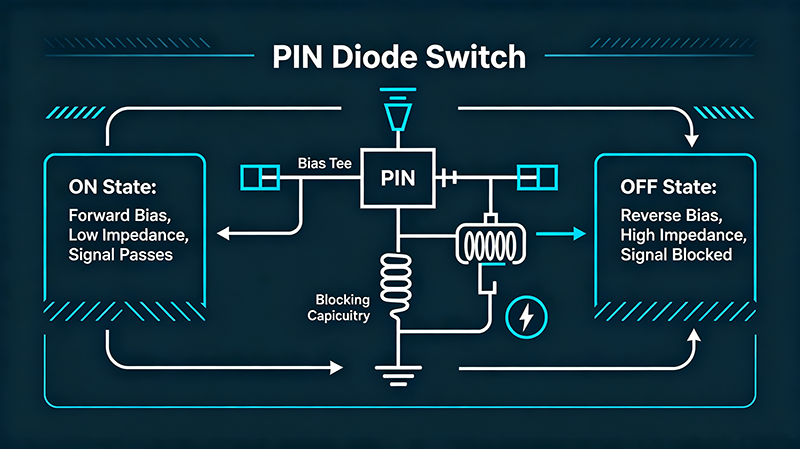






Designing high-speed PIN diode switches for RF and microwave applications requires careful attention to circuit topology, driver design, and PCB layout. Achieving nanosecond switching speeds while maintaining low insertion loss and high isolation demands systematic design approaches and optimization. This comprehensive guide provides expert techniques for designing switches that deliver maximum speed and performance.
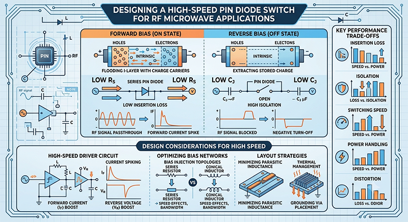
1. Define Speed Requirements
Before designing any high-speed PIN diode switch, clearly define the switching speed requirements. These specifications drive all subsequent design decisions including topology selection, diode choice, and driver circuit design.
Switching Speed Specifications
| Speed Class | Typical Switching Time | Applications |
|---|---|---|
| Ultra-High Speed | < 10 ns | Fast frequency hopping, advanced radar |
| High Speed | 10 - 100 ns | 5G TDD, phased array radar, EW |
| Medium Speed | 100 ns - 1 µs | Antenna switching, band selection |
| Standard | > 1 µs | Test equipment, simple switching |
Key Parameters to Document
- Rise Time (t_r): Time to transition from OFF to ON state
- Fall Time (t_f): Time to transition from ON to OFF state
- Propagation Delay: Time from control signal to RF output change
- Settling Time: Time for output to stabilize within specifications
- Switching Repetition Rate: Maximum switching frequency
t_total = t_driver + t_intrinsic + t_RF_settling
2. Choose Circuit Topology
The circuit topology fundamentally determines achievable switching speed, insertion loss, and isolation. Choose the topology that best matches your speed and performance requirements.
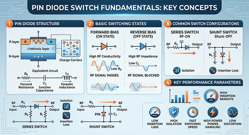
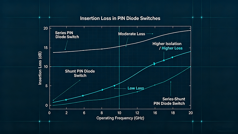
Series-Shunt Combined Topology (Recommended)
For maximum switching speed with optimal performance, the series-shunt combined topology offers the best balance of characteristics:
Insertion Loss: 10*log10(1 + Rs/2/Z0) + loss_shunt
Isolation: 20*log10(1 + Z0/2/Rs) + isolation_shunt
Why Series-Shunt for High Speed
- Faster Switching: Reduced carrier lifetime requirements due to symmetric design
- Better Isolation: Shunt diode provides additional blocking
- Lower Insertion Loss: Series diode minimizes main path loss
- Improved VSWR: Both states present matched impedances
- Higher Power Handling: Distributed voltage across both diodes
Topology Selection by Speed
Series Only
Speed: Fast (limited by single diode)
Best For: Low frequency, simple designs
Limitation: Poor high-frequency isolation
Shunt Only
Speed: Fast (single diode)
Best For: High frequency applications
Limitation: Higher drive complexity
Series-Shunt
Speed: Very Fast
Best For: Best overall performance
Advantage: Optimal balance
Bridge Configuration
Speed: Fast
Best For: Balanced differential signals
Advantage: Excellent common-mode rejection
Recommended for Ultra-High Speed
For sub-10ns switching, use the series-shunt topology with low-carrier-lifetime PIN diodes and a high-current driver circuit. This combination minimizes intrinsic switching time while maintaining performance.
3. Select PIN Diodes
PIN diode selection is critical for achieving target switching speeds. The carrier lifetime directly determines switching time and must be carefully matched to your application.
Carrier Lifetime Impact on Speed
t_off ≈ τ * ln(1 + I_F/I_R)  (turn-off time)
t_on ≈ τ * (I_F/I_R - 1) * constant  (turn-on time)
Diode Selection Criteria
- Carrier Lifetime (τ): Shorter = faster switching, but lower power handling
- Series Resistance (Rs): Lower = lower insertion loss
- Junction Capacitance (Cj): Lower = better high-frequency isolation
- Breakdown Voltage (Vbr): Higher = higher power handling
- Package Parasitics: Lower inductance = faster switching
Diode Trade-offs
| Carrier Lifetime | Switching Speed | Power Handling | Typical Application |
|---|---|---|---|
| < 10 ns | Sub-100ns | Low (< 1W) | Test, instrumentation |
| 10 - 50 ns | 100 - 500ns | Medium (1-10W) | Communications |
| 50 - 200 ns | 500ns - 2µs | High (10-100W) | Radar, base stations |
| > 200 ns | > 2µs | Very High (>100W) | High-power radar |
4. Design Driver Circuit
The driver circuit often determines overall switching speed. A well-designed driver provides fast current transitions to rapidly charge and discharge the PIN diode's intrinsic region.
High-Speed Driver Requirements
- Rise/Fall Time: Less than 20% of target switching time
- Current Capability: Sufficient to charge diode junction quickly
- Voltage Levels: Match diode forward voltage requirements
- Reverse Bias: Provide adequate negative voltage for fast turn-off
- Output Impedance: Low impedance for fast transitions
Driver Circuit Topologies
TTL/CMOS Buffer
Simple, low-cost option. Limited to slow switching. Good for sub-microsecond applications with proper design.
High-Speed Comparator
Fast transitions, adjustable current. Excellent for 10-100ns range with current limiting resistors.
Dedicated PIN Driver IC
Optimized for PIN diode switching. Built-in charge pumps, fast edges, controlled rise/fall times.
Discrete Transistor
Maximum performance flexibility. Custom current levels, fastest possible switching with proper design.
Driver Design Techniques
- Charge Pump: Generate high reverse voltage for fast carrier removal
- Current Steering: Switch between high forward and high reverse currents rapidly
- Acceleration Capacitors: Provide fast current spikes for initial switching
- Active Pull-up/Pull-down: Reduce driver output impedance for faster edges
I_F_min = Q_stored / t_on_target  (minimum for fast turn-on)
where Q_stored is the charge stored in intrinsic region
Recommended Driver ICs
For fastest switching, use dedicated PIN diode driver ICs from manufacturers like Macom, Skyworks, or Qorvo. These devices integrate charge pumps, current limiting, and optimized output stages for maximum switching performance.
5. Optimize Bias Network
The bias network must provide fast current changes to the PIN diode while maintaining RF isolation. Optimizing this network is critical for achieving target switching speeds.
Critical Bias Network Components
RF Choke Selection
- Inductance Value: High enough to present high impedance at RF frequency
- Self-Resonant Frequency: Must exceed highest operating frequency
- DC Current Rating: Must handle forward bias current
- Saturation Current: Must exceed maximum forward current
DC Blocking Capacitor Selection
- Capacitance Value: Low impedance at operating frequency
- Self-Resonant Frequency: Exceed operating frequency
- Voltage Rating: Exceed maximum reverse voltage
- ESR and ESL: Minimize for best RF performance
Bias Network Optimization
τ_bias = L_RFC / R_load (affects switching time)
To minimize bias network effects on switching speed:
- Use the smallest inductance values that still provide adequate RF isolation
- Choose quarter-wave transmission lines for frequencies above 5 GHz
- Minimize trace lengths between components
- Use parallel decoupling for multiple frequency bands
- Consider active bias circuits for fastest switching
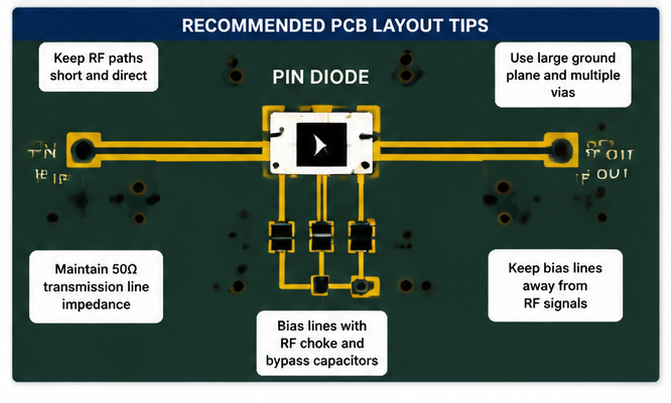
6. PCB Layout Strategies
PCB layout is crucial for high-speed PIN diode switch performance. Parasitic inductance, capacitance, and ground discontinuities can significantly degrade switching speed and RF performance.
Critical Layout Rules
Trace and Component Placement
- Minimize Trace Lengths: Each nanohenry of inductance slows switching
- Short Ground Returns: Use multiple vias to minimize ground inductance
- Direct Component Connections: Avoid long traces between key components
- Separated Analog/Digital Grounds: Prevent digital switching noise coupling
- Solid Ground Planes: Provide low-impedance return paths
Decoupling Network Layout
- Place Capacitors Within 2mm: Of device pins for effectiveness
- Use Multiple Values: 10pF + 100pF + 10nF + 1µF for broadband decoupling
- Direct Vias to Ground: Minimize parasitic inductance
- Wide Bias Traces: Reduce DC resistance and inductance
- Separate Decoupling Networks: For each diode in multi-diode circuits
High-Speed Layout Checklist
Material Selection Matters
Use low-loss, low-dispersion PCB materials like Rogers RO4003C or RT/duroid for high-frequency applications. Standard FR-4 has higher losses and less consistent dielectric properties that can degrade high-speed performance.
7. Performance Verification
After fabrication, thorough testing ensures your high-speed PIN diode switch meets all specifications. Use proper measurement techniques to verify switching speed, RF performance, and reliability.
Required Test Equipment
- Vector Network Analyzer (VNA): Measure S-parameters across frequency
- High-Speed Oscilloscope: Capture switching waveforms with sub-nanosecond resolution
- Signal Generator: Provide RF stimulus for switching tests
- Function Generator: Drive control signals with precise timing
- Spectrum Analyzer: Verify spectral purity and detect spurious signals
Key Measurements
| Measurement | Equipment | Target Parameter |
|---|---|---|
| Insertion Loss vs Frequency | VNA | < 1 dB typical |
| Isolation vs Frequency | VNA | > 40 dB |
| Switching Time | Oscilloscope | < 100 ns |
| VSWR | VNA | < 1.5:1 |
| Power Handling | Signal Generator + Power Meter | Per spec |
| Temperature Performance | Chamber + VNA | Across operating range |
Frequently Asked Questions
Conclusion
Designing high-speed PIN diode switches for RF and microwave applications requires systematic attention to circuit topology, diode selection, driver design, and PCB layout. Following the principles outlined in this guide enables switches that achieve nanosecond switching speeds while maintaining excellent RF performance.
The key to successful high-speed design is understanding the trade-offs between switching speed, power handling, insertion loss, and isolation. The series-shunt topology with optimized driver circuits typically provides the best balance of these parameters for demanding applications.
As wireless systems continue to demand faster switching for 5G, radar, and emerging applications, mastering high-speed PIN diode switch design becomes increasingly important. Use the techniques and best practices in this guide as a foundation, then optimize for your specific application requirements through simulation, prototyping, and thorough testing.
Need Expert Help with Your Switch Design?
Our engineering team can provide design review, simulation support, and optimization services for your high-speed PIN diode switch applications.
Contact Our Technical Team