The Difference Between GaAs and GaN RF Power Amplifiers
Choosing between GaAs and GaN for an RF power amplifier is one of the most common decisions RF engineers face. Both are compound semiconductors, both dominate commercial and defense RF, but they solve different problems. GaAs is mature, cheap, and ideal for moderate-power, high-volume consumer wireless. GaN delivers higher power density, efficiency, and frequency capability, but at higher cost. This guide walks through the differences in plain terms and shows when to pick each.
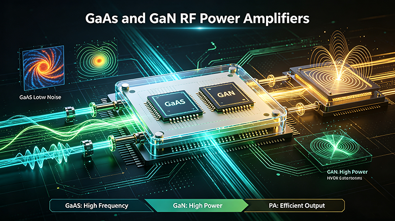
Figure 1: GaAs and GaN at a glance - voltage, power density, and typical applications
Quick answer: Choose GaAs for low-to-moderate power (< 5 W), high-volume applications such as handset PAs and Wi-Fi front ends. Choose GaN for high power (> 10 W), high frequency (> 3 GHz), high efficiency, or harsh-environment designs such as radar, EW, and satellite communications.
What Are These Two Technologies?
Gallium Arsenide (GaAs) is a III-V compound semiconductor with a mature, high-volume ecosystem. Common RF PA device structures include GaAs HBT (Heterojunction Bipolar Transistor) and GaAs pHEMT (pseudomorphic High Electron Mobility Transistor). GaAs has been the workhorse of mobile-phone PAs for decades.
Gallium Nitride (GaN) is a wide-bandgap (WBG) semiconductor. RF GaN is typically built as an AlGaN/GaN HEMT on a SiC or silicon substrate. It delivers higher breakdown voltage, higher power density, and superior thermal performance compared to GaAs.
Side-by-Side Comparison
Parameter
GaAs
GaN
Bandgap
1.42 eV
3.4 eV (wide bandgap)
Typical breakdown field
~0.4 MV/cm
~3.3 MV/cm
Operating voltage
3 – 8 V
28 – 50 V
Power density
1 – 3 W/mm
5 – 15 W/mm
Frequency capability
Up to ~50 GHz
Up to ~110 GHz
Efficiency (PAE)
35 – 55%
50 – 75%
Thermal conductivity
46 W/m·K
130 – 490 W/m·K (on SiC)
Cost per watt
Low (mature fabs)
Higher (smaller, fewer fabs)
Maturity
Very high
High and growing rapidly
How Each Technology Works
Figure 2: Cross-section comparison of GaAs HBT and AlGaN/GaN HEMT on SiC
GaAs (HBT / pHEMT)
GaAs HBTs use a heterojunction between different III-V materials (e.g. InGaP/GaAs) to improve carrier injection and frequency response. pHEMTs use a high-mobility 2-D electron gas (2DEG) for low-noise, high-frequency operation. GaAs PAs are typically operated at low DC voltages (3 – 8 V) and deliver moderate output power at excellent linearity.
GaN (AlGaN/GaN HEMT on SiC)
GaN HEMTs exploit a high-density 2DEG channel formed at the AlGaN/GaN interface. The wide bandgap allows much higher electric fields before breakdown, supporting high drain voltages (28 – 50 V). When built on SiC substrates, heat is removed very efficiently, enabling compact high-power devices.
Key Engineering Trade-offs
Figure 3: Typical PAE (Power-Added Efficiency) versus frequency for GaAs vs GaN PAs
Aspect
GaAs Strength
GaN Strength
Power density
Moderate
3–5× higher per mm
DC efficiency
Lower at high power
Higher (less DC current for same Pout)
Bandwidth
Wide for handset bands
Excellent for ultra-wideband (2–18 GHz)
Linearity
Very good (HBT)
Good (Doherty needed for high linearity)
Thermal
Needs care > 5 W
Handles high Tj without failure
Frequency limit
Excellent < 6 GHz
Better at mmWave (28, 39, 77 GHz)
Cost / availability
Mature, cheap, huge supply
Fewer fabs, but supply growing
Reliability
Field-proven over decades
Proven in defense & 5G base stations
Application Areas
Figure 4: Typical application sweet spots for GaAs vs GaN power amplifiers
Application
Preferred Technology
Why
Smartphone / cellular handset PA
GaAs
Low cost, small size, good linearity, integrated with switches
Wi-Fi 6 / 6E / 7 front-end
GaAs
Mature, cheap at 5 – 7 GHz, integrated FEMs widely available
5G / LTE base station (mMIMO)
GaN
High efficiency Doherty PAs, handles 100+ W per element
Phased-array radar (S/C/X/Ku band)
GaN
Power density + efficiency shrink the T/R module size
Electronic warfare (EW) jammers
GaN
Wide bandwidth, high Pout, robust against mismatched loads
Satellite comms (SATCOM, sat-on-move)
GaN
High efficiency reduces thermal load on small platforms
IoT / ISM-band radios
GaAs
Lowest BOM cost, sufficient power for sub-GHz links
mmWave 5G (28 / 39 GHz)
GaN or GaAs
GaN favored for base stations; GaAs for mobile handsets
How to Choose Between GaAs and GaN
Decision Factor
Pick GaAs if…
Pick GaN if…
Output power
< 5 W continuous
> 10 W continuous
Frequency
< 6 GHz dominant
> 6 GHz or mmWave
Efficiency target
> 40% acceptable
> 55% required
Thermal budget
Loose, < 60 °C ambient
Tight, sealed enclosure or aerospace
Volume
Millions per year
Tens of thousands per year
Unit cost target
< $0.50 typical
> $5 acceptable
Figure 7: Decision flow for selecting GaAs vs GaN based on power, frequency, and cost
Rule of thumb: If your PA design is destined for a smartphone, Wi-Fi router, or sub-6 GHz small cell, GaAs almost always wins on cost and integration. If the PA drives a phased-array module, a high-power EW jammer, or a satellite SSPA, GaN wins on every technical axis that matters.
Design Considerations
Figure 5: Doherty PA topology commonly used in modern GaN and high-power GaAs transmitters
Bias sequencing: GaN HEMTs need controlled gate voltages during power-up to avoid current collapse.
Packaging: GaN on SiC packages handle higher Tj (200 °C+) and higher currents than GaAs plastic packages.
Linearization: GaN PAs often use DPD or Doherty to meet 5G ACLR/EVM specs.
Thermal management: GaN can tolerate higher Tj but still benefits from copper heatsinks or cold plates.
Reliability testing: GaN follows JEDEC JESD22 and military MIL-STD qualification flows.
Common Mistakes to Avoid
Figure 8: Five recurring design pitfalls when choosing between GaAs and GaN
Choosing GaN when cost dominates. GaN's BOM savings rarely beat GaAs at < 2 W.
Choosing GaAs for high power. Efficiency drops and thermal issues explode above ~5 W.
Ignoring linearization. Both technologies need DPD or ET for modern modulation formats.
Forgetting gate protection. GaN HEMTs are very sensitive to gate overvoltage; always include clamping.
Mixing bias voltages. GaAs runs at 3–5 V, GaN at 28–50 V — DC-DC design is very different.
Future Trends
Figure 6: Typical saturated output power versus frequency for GaAs vs GaN PAs
GaN-on-silicon
Cost roadmap: GaN grown on Si substrates may eventually rival GaAs cost.
mmWave GaN
Needed for 5G/6G base stations at 28, 39, 77 GHz.
GaN IC integration
Monolithic GaN-on-SiC ICs combine PA, switch, and LNA on one die.
Improved GaAs HBT
InP HBT and advanced GaAs processes push handset efficiency.
Heterogeneous packaging
GaAs front-end + GaN PA + CMOS controller in multi-chip modules.
Frequently Asked Questions
Is GaN always better than GaAs for RF power amplifiers?
No. GaN is better for high power, high efficiency, and high frequency. But GaAs remains cheaper and highly integrated for low-to-moderate power applications such as handset and Wi-Fi PAs.
Can GaN replace GaAs in smartphones?
Not yet. GaN's higher voltage and lower capacitance don't match the integrated front-end modules (FEMs) used in smartphones, where GaAs still dominates on cost and integration density.
Why is GaN more expensive than GaAs?
Fewer fabs, smaller wafer sizes, and the cost of SiC substrates all contribute. As GaN-on-Si matures, costs are expected to drop.
Which technology is more reliable?
Both are field-proven. GaAs has decades of high-volume reliability data. GaN's reliability has been validated by defense and telecom deployments over 15+ years.
Does GaN always need a heatsink?
GaN tolerates higher junction temperatures and concentrates power in a smaller die, but for sustained high power it still needs careful thermal management, often integrated into the package.
Which is better for mmWave (28+ GHz)?
GaN offers superior power density at mmWave, but GaAs is widely used for cost-sensitive mmWave PAs. The choice depends on whether power or cost dominates.
Key Takeaways
• GaAs is mature, cheap, and the right choice for low-to-moderate power, high-volume wireless PAs.
• GaN delivers 3–5× higher power density, higher efficiency, and better thermal performance.
• Choose GaAs for < 5 W in handsets, Wi-Fi, IoT; choose GaN for > 10 W in radar, EW, satellite, base stations.
• GaN is becoming more affordable and is expanding into mmWave and 5G/6G infrastructure.
• Both technologies rely on advanced linearization (DPD, Doherty) for modern modulation formats.
Discover how RF power amplifiers enable military communication systems. Learn roles in tactical radios, EW, radar, SATCOM, SDR, and phased arrays, plus GaN vs GaAs trade-offs and design tips.
Solid state power amplifiers explained — what an SSPA is, how it works, the main types (LDMOS, GaN, GaAs), key specifications like gain, efficiency and linearity, and how SSPA compares to TWTAs and tube amplifiers.
Learn how power amplifiers work, explore the different amplifier classes, understand their key specifications, and discover why high-performance RF and microwave power amplifiers are essential for modern communication, radar, testing, broadcasting, and industrial applications.
Aug 20 ,26
About the Author — MeiXun Team
Wang
Chief Engineer Wang
High-tech Enterprise, Feifeng Talent
Chief Engineer Wang graduated with a master's degree in high-power microwave from the Institute of Electronics, University of Chinese Academy of Sciences.
View Full Profile
Wang
Chief Engineer Wang
High-tech Enterprise, Feifeng Talent
Chief Engineer Wang graduated with a master's degree in high-power microwave from the Institute of Electronics, University of Chinese Academy of Sciences.
In the same year, he joined CETC 40/41 for work and study. He has been committed to the design and development of microwave switches for a long time.
He has applied for 27 patents as the first inventor in the microwave switch field, with 6 authorized invention patents and 14 utility model patents.
The products he developed cover various application platforms such as civilian testing, vehicle-mounted, shipborne, airborne, and missile-borne.