Solid State Power Amplifiers: Working Principle, Types & Applications

A solid state power amplifier (SSPA) is an RF amplifier that uses semiconductor transistors — typically LDMOS, GaN, or GaAs — to deliver high output power. Solid state amplifiers have largely replaced traveling-wave tubes (TWTs) in modern radar, satellite, wireless, and electronic-warfare systems thanks to their reliability, small size, and ease of integration.

Quick Answer

A solid state power amplifier is a multi-stage transistor amplifier that boosts an RF input signal to a useful output level — typically tens to hundreds of watts CW or kilowatts pulsed. Modern SSPAs use GaN HEMT devices for the highest power density and efficiency, or LDMOS for sub-6 GHz cellular and broadcast. They offer long lifetimes, low-voltage operation, and graceful degradation, in contrast to vacuum tubes.

What Is a Solid State Power Amplifier?

What Is a Solid State Power Amplifier

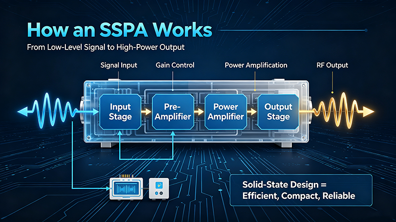
An SSPA is a multi-stage amplifier chain built from solid-state transistors. Each stage provides gain; multiple stages combine to reach the desired output power. Inside a single SSPA module, you typically find:

  • Input matching network: transforms 50 Ω to the optimal impedance for the first transistor.
  • Driver stage: small-signal gain block that brings input to a level the final stage can amplify.
  • Power stage: large transistors operating near P1dB or saturation.
  • Combiner / splitter: combines outputs of multiple transistors in parallel.
  • Output matching network: transforms the device impedance back to 50 Ω.
  • Bias and protection circuitry: supplies DC, monitors temperature, current, and VSWR.

How an SSPA Works

How an SSPA Works

The fundamental principle is the same as any transistor amplifier: a small input RF signal modulates the current through the transistor, producing a larger replica at the output. The ratio of output power to input power is the gain (in dB), and the efficiency is the ratio of RF output power to DC input power.

In an SSPA, multiple transistors work together to deliver high total power:

  • Parallel combining: several transistors drive a common output through a Wilkinson or hybrid combiner.
  • Cascaded gain: each stage provides 10 – 15 dB of gain; multiple stages reach 50 – 60 dB total.
  • Linearization: digital predistortion (DPD) corrects AM/AM and AM/PM distortion.

Key Specifications

Specification Meaning
Frequency Range Operating band
Output Power (Psat) Maximum CW output
Gain Output ÷ input (dB)
Power-Added Efficiency (PAE) (Pout − Pin) / PDC
Linearity (ACPR / EVM) Distortion relative to input
Operating Class A, AB, B, C, F, Doherty
Supply Voltage DC rail (28V, 48V typical)
Cooling Conduction, forced air, liquid
VSWR Tolerance Load mismatch survival (typically 3:1 – 5:1)
MTBF Mean time between failures

Semiconductor Technologies

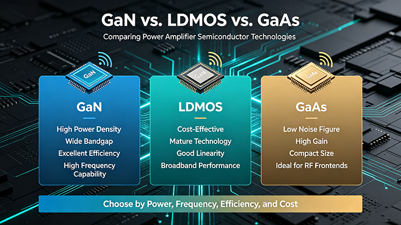
GaN

GaN HEMT

Gallium-nitride high-electron-mobility transistors. Highest power density, highest efficiency, broadband operation from VHF to W-band. Modern choice for radar and EW.

LDMOS

LDMOS FET

Laterally-diffused MOSFET. Dominant in sub-6 GHz cellular base stations and broadcast transmitters. Excellent efficiency with DPD, mature supply chain.

GaAs

GaAs pHEMT

Gallium-arsenide pseudomorphic HEMT. Lower power but excellent noise and linearity; used in drivers, MMICs, and microwave links.

SiGe

SiGe HBT

Silicon-germanium heterojunction bipolar transistor. Integrated on standard CMOS processes for compact, low-cost amplifiers up to mmWave.

InP

InP HBT / HEMT

Indium-phosphide. Highest frequency and lowest noise, but expensive. Used in optical drivers, mmWave, and niche EW.

SiC

SiC MESFET

Silicon-carbide. High temperature and high voltage capability, used in rugged industrial RF applications.

GaN vs. LDMOS vs. GaAs

GaN vs. LDMOS vs. GaAs

Parameter GaN HEMT LDMOS GaAs pHEMT
Frequency DC – 100 GHz+ up to ~6 GHz DC – 60 GHz
Power Density Very high (5 – 10 W/mm) High (1 – 2 W/mm) Moderate (0.5 – 1 W/mm)
Efficiency 65 – 75 % (Doherty) 50 – 60 % (DPD) 30 – 45 %
Breakdown Voltage 100 – 200 V 50 – 80 V 10 – 20 V
Supply Voltage 28 – 50 V 28 – 50 V 5 – 12 V
Cost / Watt Moderate Low Moderate
Best For Radar, EW, satcom Cellular, broadcast Drivers, MMIC

Amplifier Operating Classes

  • Class A: bias at the center of the device's I-V curve. Linear but low efficiency (≤ 50 %).
  • Class AB: small bias offset from Class B. Linear with higher output power than Class A.
  • Class B: bias at cutoff. 78 % theoretical efficiency, but more distortion.
  • Class C: bias below cutoff. High efficiency, used only for constant-envelope signals.
  • Class F / Inverse F: harmonic-tuned for > 90 % efficiency at the cost of bandwidth.
  • Doherty: carrier + peaking amplifier architecture for high efficiency at backed-off power.

SSPA vs. TWTA vs. Tube Amplifiers

SSPA vs. TWTA vs. Tube Amplifiers

SSPA

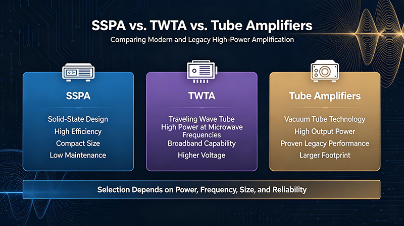
  • + Long lifetime (50,000 – 100,000 hr)
  • + Low voltage, safe to operate
  • + Compact, no warm-up
  • + Modular, graceful degradation
  • − Lower peak power per unit
  • − Less efficient at saturation

TWTA

  • + Very high output power (kW)
  • + Wide instantaneous bandwidth
  • + High efficiency at saturation
  • − Limited lifetime (10,000 – 20,000 hr)
  • − High voltage, X-ray shielding
  • − Single point of failure

Vacuum Tube

  • + Extremely high peak power
  • + Mature technology
  • + Tolerant of VSWR mismatch
  • − Very heavy and bulky
  • − Slow warm-up
  • − High operating voltage

Linearization Techniques

Modern SSPAs use linearization to meet strict spectral-emission masks for 4G/5G and Wi-Fi.

  • Digital predistortion (DPD): applies an inverse non-linearity in the digital baseband. Most common technique.
  • Feed-forward cancellation: subtracts distortion products using a secondary amplifier.
  • Envelope tracking: dynamically adjusts supply voltage to match envelope.
  • Predistortion with memory:
  • Volterra-series DPD handles memory effects.

Thermal Management

A typical GaN amplifier converts 30 – 50 % of DC input into heat. Removing that heat is critical:

  • Conduction cooling: bolted to a heat sink or cold plate.
  • Forced air: integrated fans or system airflow.
  • Liquid cooling: water or refrigerant for high-power radar and EW.
  • Heat pipes / vapor chambers: spread heat from small hot spots.

Always verify junction temperatures against the manufacturer's derating curves. Every 10 °C rise roughly halves the median lifetime.

Rule of Thumb: For a 100 W CW SSPA with 50 % efficiency, expect 100 W of waste heat. Plan your cooling and airflow accordingly.

Protection and Monitoring

Most modern SSPAs include self-protection and telemetry:

  • Over-temperature shutdown if the case or junction exceeds limits.
  • Over-current and over-voltage protection on the DC rail.
  • VSWR foldback reduces power when load mismatch exceeds a threshold.
  • RF input overdrive detection shuts down or attenuates.
  • Status telemetry (Ethernet, RS-232, CAN) reports health to the host system.

Real-World Applications

  • Cellular base stations: LDMOS SSPAs dominate 4G/5G macro cells at 700 MHz – 4 GHz.
  • Radar: GaN SSPAs deliver 10 – 100 W per module in active phased arrays.
  • Satellite communication: SSPA modules inside satellite payloads and ground terminals.
  • Electronic warfare: broadband GaN SSPAs for jammers and DRFM-driven threats.
  • Broadcast: LDMOS transmitters in VHF/UHF TV and FM radio.
  • Medical: MRI RF amplifiers and surgical generators.
  • Scientific: particle accelerator RF drivers and plasma sources.

Choosing the Right SSPA

  1. Define frequency band, bandwidth, and modulation.
  2. Specify required output power (Psat and linear power).
  3. Set minimum efficiency target for thermal design.
  4. Choose semiconductor technology (GaN, LDMOS, GaAs).
  5. Verify linearity / EVM / ACPR against regulatory mask.
  6. Confirm VSWR tolerance and protection features.
  7. Validate cooling method (conduction, air, liquid).
  8. Check control interface and telemetry compatibility.

Common Mistakes

  • Under-sizing cooling: amplifiers derate or fail prematurely.
  • Ignoring load mismatch: VSWR > 3:1 can damage the final stage.
  • Running too far into compression: degrades linearity and spectral mask.
  • Forgetting DPD or linearization: non-linear output fails regulatory tests.
  • Mixing tech in one chain: GaN driver into LDMOS final can cause instability.

Key Takeaways

  • An SSPA uses semiconductor transistors (GaN, LDMOS, GaAs) to deliver high RF power.
  • GaN offers the highest power density and efficiency; LDMOS dominates sub-6 GHz; GaAs serves drivers.
  • SSPAs offer long life, low voltage, and modular graceful degradation.
  • Linearization (DPD) is essential for modern wireless systems.
  • Thermal management is as important as electrical design.

Frequently Asked Questions

What does SSPA stand for?

SSPA stands for Solid State Power Amplifier. It uses semiconductor transistors to amplify RF signals, as opposed to vacuum tubes or traveling-wave tubes.

SSPA vs. TWTA — which is better?

SSPAs are smaller, lighter, more reliable, and run on low voltage. TWTAs deliver higher peak power and wider bandwidth, but are bulkier and have shorter lifetimes. For most modern applications, SSPAs have replaced TWTAs.

What is GaN's main advantage?

GaN HEMTs offer the highest power density, highest breakdown voltage, and best efficiency of any semiconductor technology, especially above 1 GHz and at high voltage.

What is PAE?

Power-Added Efficiency (PAE) = (Pout − Pin) / PDC. It measures how efficiently the amplifier converts DC power into additional RF output.

How is SSPA linearity improved?

Digital predistortion (DPD) is the dominant technique. It applies an inverse distortion in the baseband so that the overall output is linear. Feed-forward and envelope tracking are also used.

  • The Ultimate Guide to Power Amplifiers: Discover the Benefits
    Learn how power amplifiers work, explore the different amplifier classes, understand their key specifications, and discover why high-performance RF and microwave power amplifiers are essential for modern communication, radar, testing, broadcasting, and industrial applications.
    Aug 20 ,26

About the Author — MeiXun Team

Wang

Chief Engineer Wang

High-tech Enterprise, Feifeng Talent

Chief Engineer Wang graduated with a master's degree in high-power microwave from the Institute of Electronics, University of Chinese Academy of Sciences.

View Full Profile
Wang

Chief Engineer Wang

High-tech Enterprise, Feifeng Talent

Chief Engineer Wang graduated with a master's degree in high-power microwave from the Institute of Electronics, University of Chinese Academy of Sciences.

In the same year, he joined CETC 40/41 for work and study. He has been committed to the design and development of microwave switches for a long time.

He has applied for 27 patents as the first inventor in the microwave switch field, with 6 authorized invention patents and 14 utility model patents.

The products he developed cover various application platforms such as civilian testing, vehicle-mounted, shipborne, airborne, and missile-borne.

RF Microwave Switch RF Switch Coaxial Switch PIN Diode Switch Low Noise Amplifier Waveguide Switch PIN Switch Microwave Switch