As wireless systems march toward
6G, operating frequencies are climbing into the
sub-THz range (140–300 GHz), bandwidths are expanding, and link budgets are tighter than ever. The
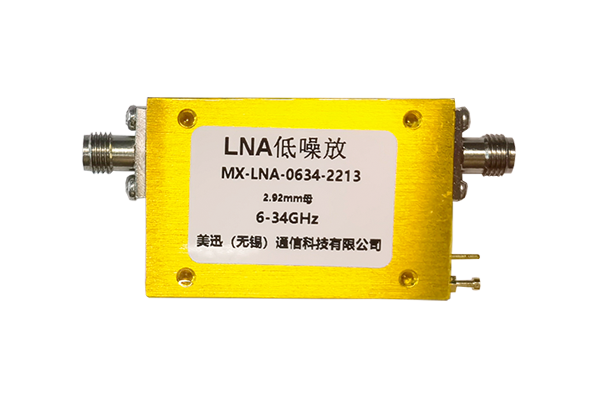
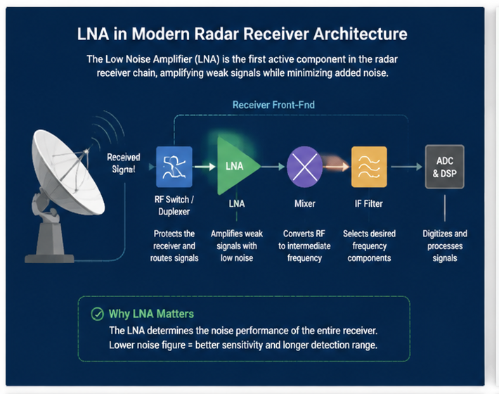
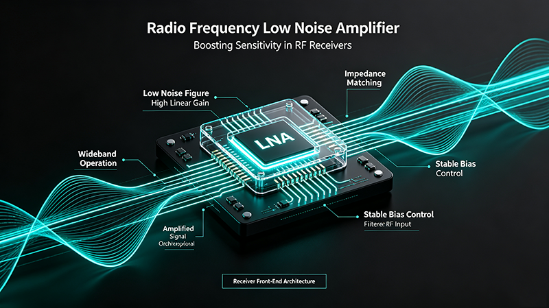
low noise amplifier (LNA) — the first active stage in any receiver — increasingly defines system sensitivity. This guide explores the semiconductor, packaging, and architectural trends shaping the next generation of mmWave LNAs.
1. Why mmWave 6G Demands Better LNAs
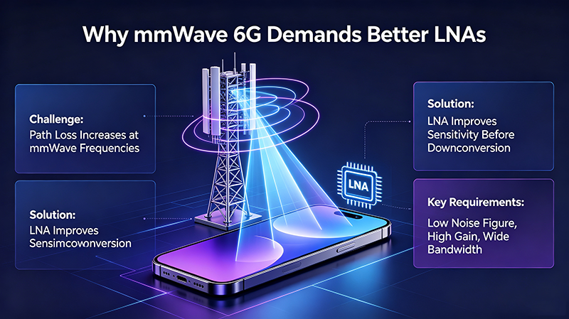
Every link-budget equation starts with the LNA. As we move from sub-6 GHz 5G into mmWave 6G, several forces compress receiver sensitivity:
-
Higher path loss at mmWave frequencies reduces received power.
-
Wider bandwidths (up to 2 GHz in 6G) increase integrated noise.
-
Phased-array architectures require LNAs in every element — driving power and area efficiency.
-
Heterogeneous networks demand concurrent multi-band reception.
-
AI-defined waveforms need high linearity to preserve complex modulations.
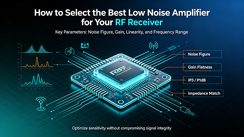
To compensate, mmWave 6G LNAs must deliver noise figures below 2 dB at 28–140 GHz, > 20 dB gain, and IP1dB above −15 dBm — simultaneously.
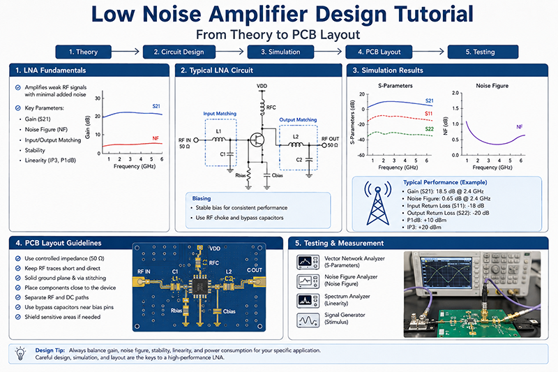
2. Key LNA Performance Metrics
-
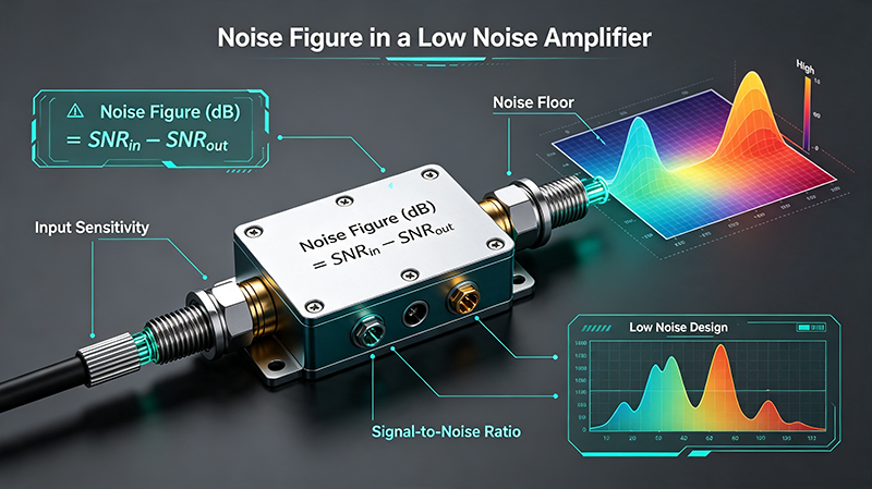
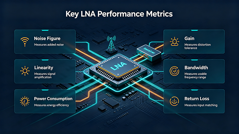
Noise Figure (NF) — the dominant metric. Lower NF means better sensitivity.
-
Gain (S21) — typically 15–25 dB per stage.
-
Linearity — P1dB and OIP3 must be high enough for the modulation scheme.
-
Bandwidth — instantaneous RF bandwidth, not just center frequency.
-
Power consumption — critical for battery-powered mobile and edge devices.
-
Stability — k-factor and μ stability across temperature and process.
-
Reverse isolation — reduces LO leakage and improves filter Q.
Cascaded NF rule: Friis' equation shows the first stage dominates system NF. A 2 dB LNA in front of a 10 dB mixer contributes only ~0.4 dB to the cascaded noise.
3. Semiconductor Technologies Compared
|
Technology
|
Best NF @ 30 GHz
|
fT / fmax
|
Power
|
Integration
|
Best Use
|
|
SiGe HBT
|
1.5–2.0 dB
|
300–500 GHz
|
Medium
|
High
|
mmWave 5G/6G, automotive radar
|
|
GaAs pHEMT
|
1.0–1.5 dB
|
150 GHz
|
Medium
|
Medium
|
Satellite, point-to-point
|
|
InP HBT/HEMT
|
0.7–1.2 dB
|
500–1000 GHz
|
Low
|
Low
|
Sub-THz, scientific instruments
|
|
GaN-on-SiC
|
1.5–2.5 dB
|
150 GHz
|
High
|
Medium
|
High-power, defence, radar
|
|
SOI CMOS
|
2.5–3.5 dB
|
200 GHz
|
Low
|
Very high
|
Mass-market mobile, beamforming
|
|
Bulk CMOS 28 nm
|
3.0–4.0 dB
|
200 GHz
|
Low
|
Very high
|
Cost-sensitive consumer
|
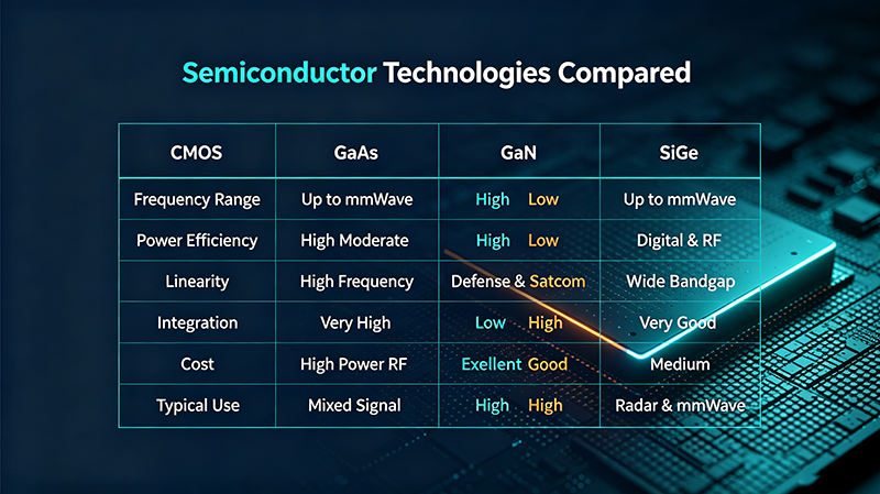
Technology Trade-off: SiGe HBT offers the best balance of NF, integration, and cost for mmWave 6G. InP wins on raw noise but loses on integration and wafer cost. SOI CMOS dominates where millions of LNAs are needed per device.
4. Emerging Materials & Devices
Beyond mainstream SiGe and CMOS, several material platforms are emerging for sub-THz LNAs:
-
InGaAs/InP HBT — sub-1 dB NF at 140 GHz. Foundational for 6G research platforms.
-
Graphene FETs — high mobility, but low current density limits gain.
-
2D materials (MoS2, hBN) — ultra-thin channels for future heterogeneous integration.
-
GaN-on-Si — lower cost GaN for mass-produced mmWave front-ends.
-
Quantum-well & quantum-dot devices — research-stage, but promising for sub-THz.
5. Architectural Innovations
5.1 Common-Base / Cascode Stages
The cascode (common-emitter + common-base) remains the workhorse mmWave topology — offering high gain, good isolation, and stable operation. New bias-network techniques minimize NF without sacrificing linearity.
5.2 Noise-Cancelling LNAs
Noise-cancelling architectures use a parallel auxiliary path to subtract the noise of the matching network. They achieve simultaneous wideband input match and low NF — critical for multi-band 6G radios.
5.3 Distributed (Traveling-Wave) LNAs
Distributed LNAs provide flat gain over multi-octave bandwidths, ideal for software-defined radios and ultra-wideband 6G waveforms.
5.4 Stacked-FET LNAs
Stacking multiple FETs in series increases breakdown voltage and improves linearity for higher-power phased-array elements.
5.5 Digital Predistortion & AI Tuning
Adaptive bias and on-chip digital calibration compensate for process, voltage, and temperature (PVT) variation — enabling reliable mmWave LNAs in volume production.
6. Packaging & Integration Trends
Packaging is often the limiting factor for mmWave LNA performance. Key trends include:
-
Wafer-level chip-scale packaging (WLCSP) — minimizes parasitic inductance.
-
Fan-out wafer-level packaging (FOWLP) — supports phased-array tile integration.
-
Embedded-die organic substrates — low-cost high-density mmWave modules.
-
3D heterogeneous integration — stacking SiGe, CMOS, and III-V dies in one package.
-
Antenna-in-package (AiP) — co-integrating antennas with LNAs for < 1 cm2 6G modules.
6G mmWave LNA target spec (2030 roadmap):
Frequency: 140 - 300 GHz
Noise Figure: < 1.8 dB Gain: > 22 dB
P1dB: > -12 dBm
Power: < 15 mW per element Supply: 0.8 V Area: < 0.15 mm^2 per stage Integration: 64 - 1024 elements per array
7. Top 6 Technology Trends
TREND 01
SiGe HBT Dominance
Advanced SiGe HBT nodes (130 nm/90 nm) deliver sub-2 dB NF up to 140 GHz with high yield, making them the leading choice for sub-THz 6G LNAs.
TREND 02
Heterogeneous 3D Integration
Stacking InP, SiGe, and CMOS in 3D packages brings the best of each technology — lowest NF plus highest integration density.
TREND 03
AI-Driven Calibration
On-chip machine-learning engines dynamically tune bias and matching to maintain NF across temperature and process variation.
TREND 04
Antenna-in-Package (AiP)
Integrated antenna arrays co-packaged with LNAs shrink 6G modules to fingernail size while maintaining multi-GHz bandwidth.
TREND 05
Sub-THz Operation
LNAs designed for 140–300 GHz using InP and SiGe BiCMOS are moving from research labs to early commercial prototypes.
TREND 06
Green Low-Power Design
Sub-1 V supplies and adaptive biasing cut LNA power consumption by 60%, supporting sustainable 6G infrastructure.
8. Application Landscape
-
6G mobile handsets — phased-array LNAs in AiP modules at 140+ GHz.
-
Satellite megaconstellations — Ka/Ku-band LNAs with sub-1 dB NF for high-throughput links.
-
Automotive radar — 77/79 GHz SiGe LNAs in ADAS and autonomous driving.
-
AR/VR wearables — ultra-low-power mmWave LNAs for immersive connectivity.
-
Industrial sensing — 60 GHz LNAs in high-resolution radar and gesture recognition.
-
Scientific instruments — InP LNAs in radio-astronomy and spectroscopy.
9. Remaining Challenges
-
Cost vs. performance — InP and GaN outperform but cost 10–100× more than CMOS.
-
Thermal density — phased arrays concentrate heat in tiny footprints.
-
Modeling accuracy — sub-THz device models still lag behind measurement data.
-
Test & characterization — S-parameter and noise measurements above 110 GHz require specialized equipment.
-
Supply chain maturity — 6G component ecosystem is still consolidating.
10. Frequently Asked Questions
Q1: What is the target noise figure for a 6G mmWave LNA?
For 28–60 GHz, < 2.0 dB is typical. For 140–300 GHz sub-THz, the target is < 3.5 dB given current technology limits.
Q2: Will CMOS LNAs replace SiGe HBT in 6G?
CMOS will dominate in highly integrated mobile devices. SiGe HBT will lead where lowest NF and linearity matter most — base stations, satellite, and sub-THz links.
Q3: How does beamforming affect LNA design?
Phased arrays need hundreds to thousands of LNAs — each with tight power, area, and uniformity requirements. This drives aggressive use of AiP and wafer-scale integration.
Q4: Is GaN suitable for LNA use?
GaN excels in high-power transmit and radar applications. For LNAs, its NF is higher than SiGe or InP, so it is reserved for rugged defense systems where power matters more than absolute NF.
Q5: What frequency will 6G use?
Initial 6G deployments will use sub-7 GHz and mmWave bands up to 60 GHz. Research is targeting 140–300 GHz sub-THz for later phases.
Q6: How important is packaging for mmWave LNAs?
Critical. Package parasitics can add 0.5–1.0 dB of NF at mmWave. AiP, WLCSP, and 3D integration are mandatory for sub-THz performance.
11. Conclusion
The race to 6G is reshaping low noise amplifier design. SiGe HBT will likely dominate sub-THz LNAs through the end of the decade, complemented by SOI CMOS for mobile and InP HBT for the lowest-noise scientific applications. Meanwhile, heterogeneous 3D integration, AI-driven calibration, and antenna-in-package architectures will define the next wave of mmWave LNA innovation. Engineers who understand these technology trends today will build the receivers that power tomorrow's 6G networks.