

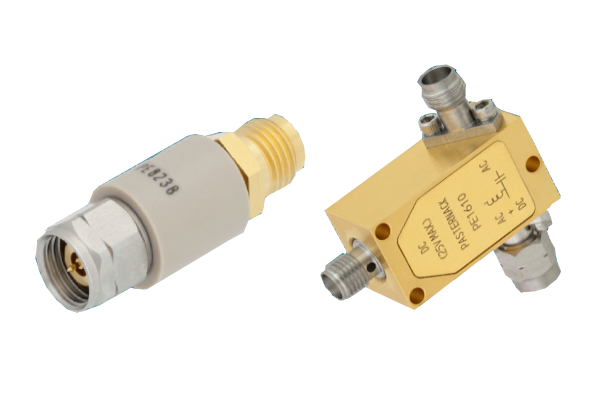
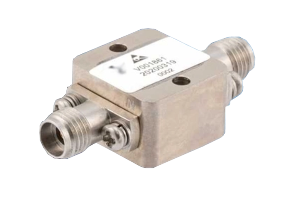
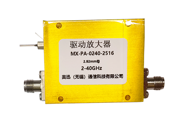



The complete guide to Low Noise Amplifiers (LNAs): technical principles, applications, selection criteria, and leading manufacturers for 5G, radar, satellite, and SDR systems.
Sep 18 ,26


5G communication testing, wireless terminal automated testing
Aerospace communication systems
Precision measurement equipment, radio frequency signal control of radar transmitters
Communication and navigation systems
Optical communication module-related testing
Interconnection of wireless communication base stations
A Low Noise Amplifier (LNA) is one of the most critical building blocks in RF and microwave systems. Whether you're designing wireless communication equipment, satellite receivers, radar systems, IoT devices, GPS modules, or test instruments, the LNA largely determines the receiver's sensitivity and overall signal quality.
This comprehensive tutorial explains the complete Low Noise Amplifier design process, covering theoretical fundamentals, component selection, impedance matching, stability analysis, bias network design, simulation, PCB layout techniques, and testing practices. Following these guidelines will help engineers develop high-performance LNAs with low noise figure, high gain, and excellent stability.
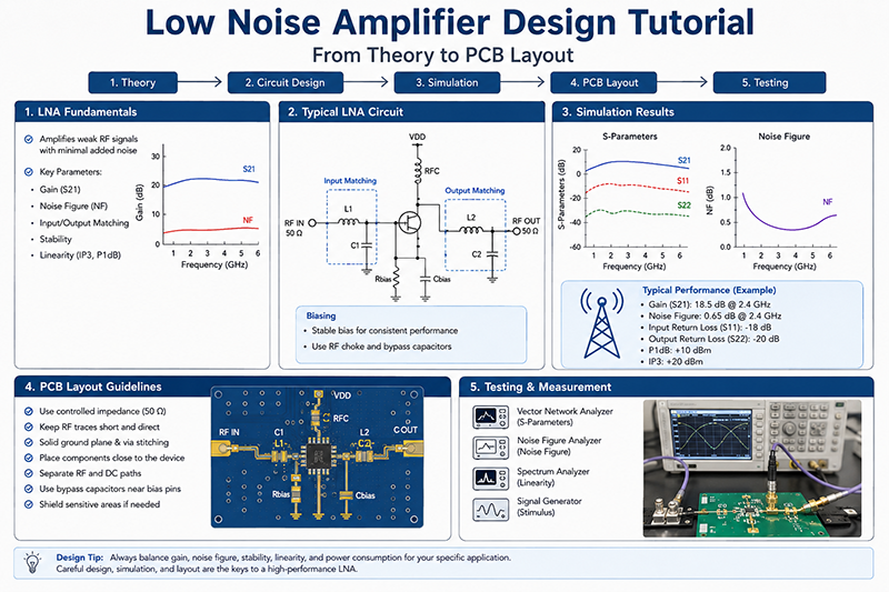
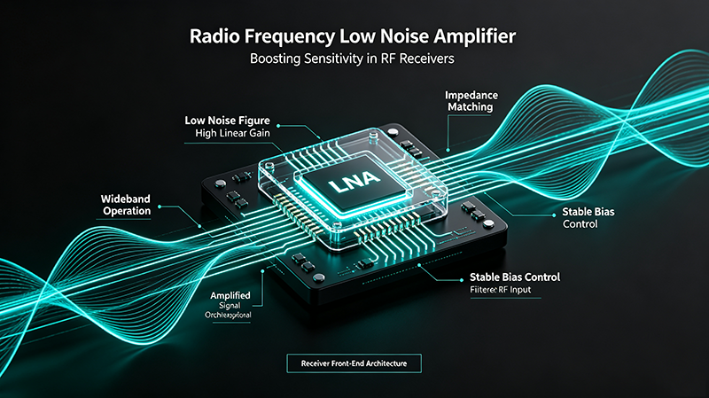
A Low Noise Amplifier is an RF amplifier designed to amplify extremely weak signals while introducing as little additional noise as possible. It is typically positioned immediately after the antenna in the receiver chain.
Gain represents the amplification capability of the LNA and is usually expressed in dB.
Typical Gain Range:
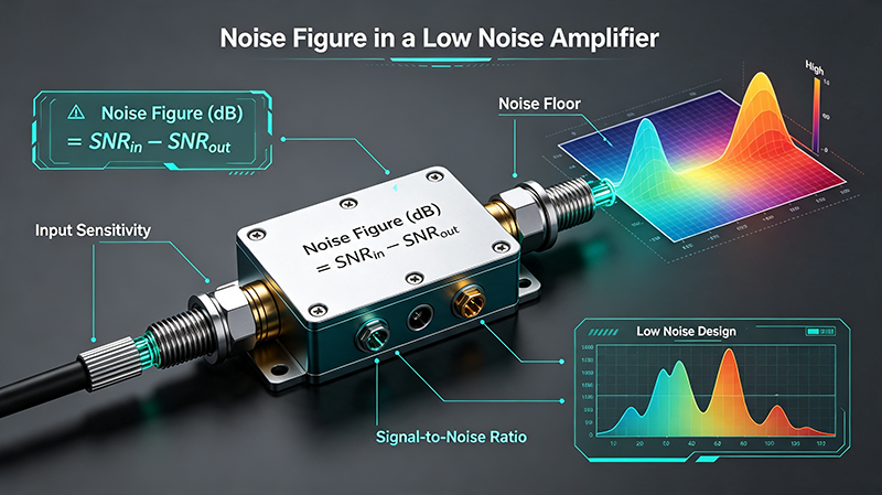
Noise Figure measures how much noise the amplifier adds to the incoming signal.
Lower NF results in higher receiver sensitivity.
| Application | Typical Noise Figure |
|---|---|
| Consumer Wireless | 1–2 dB |
| Cellular Base Stations | 0.6–1 dB |
| Satellite Receivers | 0.3–0.8 dB |
| Scientific Instruments | Below 0.5 dB |
An LNA must amplify weak signals without generating excessive distortion.
Important linearity parameters include:
RF amplifiers can oscillate if not properly designed. Stability analysis ensures reliable operation across all frequencies.
Engineers commonly evaluate:
The active device determines much of the amplifier's overall performance.
| Technology | Advantages | Applications |
|---|---|---|
| GaAs pHEMT | Ultra-low noise | Satellite, Radar |
| GaN HEMT | High power handling | Military Systems |
| SiGe HBT | Excellent integration | 5G, IoT |
| CMOS RF | Low cost | Consumer Electronics |
Manufacturers typically provide:
A stable bias network ensures consistent amplifier performance over temperature and supply voltage variations.
Impedance matching maximizes power transfer while minimizing reflections.
The input network is usually optimized for minimum noise figure rather than maximum gain.
Common matching structures include:
The output network is generally optimized for gain, output power, and linearity.
The Smith Chart remains one of the most valuable tools for RF engineers.
It helps visualize:
Modern RF design relies heavily on simulation software before PCB fabrication.
Popular tools include:
Typical simulations include:
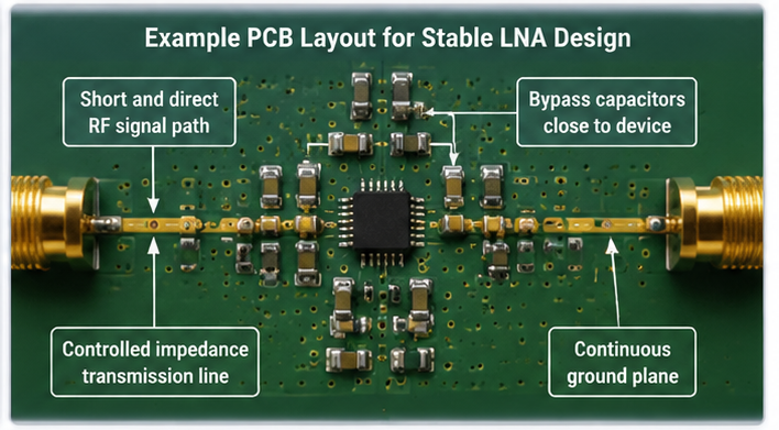
Excellent circuit design can still fail if PCB layout is poor. RF PCB design significantly impacts gain, stability, and noise performance.
Shorter traces reduce insertion loss and unwanted parasitic effects.
Use an uninterrupted RF ground plane with numerous stitching vias.
Design 50 Ω microstrip or coplanar waveguide traces according to PCB stack-up.
Avoid running DC supply lines parallel to RF transmission lines.
Metal shielding cans help reduce EMI and external interference.
Although many LNAs consume relatively low power, thermal stability remains important for maintaining gain and noise performance.
Recommended techniques include:
After fabrication, validate amplifier performance using calibrated RF test equipment.
| Measurement | Equipment |
|---|---|
| Gain | Vector Network Analyzer |
| Noise Figure | Noise Figure Analyzer |
| Output Power | Spectrum Analyzer |
| Linearity | Signal Generator + Spectrum Analyzer |
| Stability | Network Analyzer |
LNAs are widely deployed across modern RF and microwave systems.
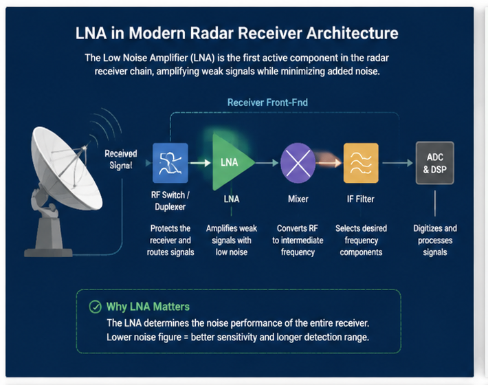
Placing the LNA at the front end minimizes the impact of subsequent stage noise, preserving receiver sensitivity according to Friis' noise equation.
Most commercial RF receivers target 0.5–2 dB, while premium satellite and scientific systems often achieve below 0.5 dB.
Not always. Designers typically balance gain, noise figure, stability, bandwidth, and linearity based on application requirements.
At microwave frequencies, parasitic capacitance, inductance, and coupling from PCB traces can significantly alter circuit behavior, making layout an essential part of the design process.
Designing a high-performance Low Noise Amplifier requires a thorough understanding of RF theory, transistor characteristics, impedance matching, stability, biasing, simulation, and PCB layout. By carefully optimizing each stage—from selecting the appropriate active device to implementing controlled-impedance routing and rigorous validation—you can achieve an LNA with exceptional gain, low noise figure, excellent linearity, and robust stability.
Whether you are developing wireless communication systems, satellite receivers, radar platforms, or IoT devices, following proven LNA design practices will enhance receiver sensitivity, improve overall RF performance, and ensure reliable operation in demanding environments.



High-tech Enterprise, Feifeng Talent
Chief Engineer Wang graduated with a master's degree in high-power microwave from the Institute of Electronics, University of Chinese Academy of Sciences.
View Full Profile