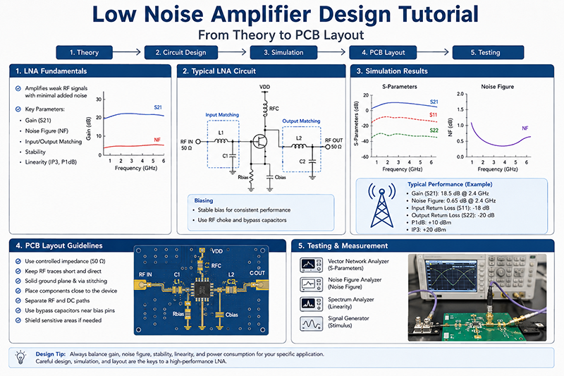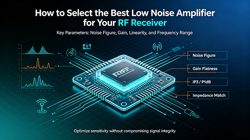






Oscillation in Low Noise Amplifiers is one of the most challenging issues faced by RF engineers. Even carefully designed circuits can oscillate under certain conditions, degrading performance and potentially causing system failure. This comprehensive guide provides systematic techniques for identifying, analyzing, and eliminating oscillations in LNA circuits.
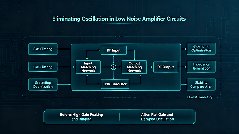
Understanding LNA Oscillation
LNA oscillation occurs when the amplifier circuit satisfies the Barkhausen stability criteria: unity loop gain at a specific phase shift (typically 0 or 360 degrees). Understanding the mechanisms that cause oscillation is essential for effective elimination.
|Loop Gain| = 1 and Phase = 360n (n = 0, 1, 2...)
Common Oscillation Types in LNAs
| Oscillation Type | Frequency | Root Cause |
|---|---|---|
| Low Frequency | < 100 MHz | Power supply feedback, bias network coupling |
| RF/VHF | 100 MHz - 1 GHz | Input/output coupling, grounding issues |
| Microwave | > 1 GHz | Package resonances, matching network instability |
| Parasitic | Various | PCB traces, component parasitics |
Stability Analysis Fundamentals
Before eliminating oscillation, engineers must understand stability analysis methods. The Rollet stability factor (K) and stability measurement (mu) provide quantitative measures of circuit stability.
K = (1 - |S11|^2 - |S22|^2 + |D|^2) / (2|S12*S21|)
where D = S11*S22 - S12*S21
Stability Criteria
Unconditional Stability Requirements
- K > 1 (Rollet stability factor)
- B1 > 0 (B1 stability factor)
- Mu > 1 (Stability parameter)
- |S11| < 1 and |S22| < 1 (Input/output match)
Identifying Oscillation Sources
Accurate identification of oscillation sources is critical for effective remediation. Different oscillation types require different solutions, so proper diagnosis is essential.
Systematic Diagnosis Process
- Observe Symptoms: Check for abnormal gain, noise figure degradation, or output distortion
- Frequency Analysis: Use spectrum analyzer to identify oscillation frequency
- Bias Variation: Vary drain voltage/current to observe stability changes
- Input/Output Termination: Test with different source/load impedances
- Temperature Testing: Monitor stability across temperature range
- Substitute Components: Replace suspected problematic components
Common Oscillation Sources
Typical Problem Areas
- Power Supply Coupling: Inadequate decoupling allows RF feedback through supply lines
- Input/Output Coupling: Insufficient isolation between input and output
- Ground Loops: Multiple ground paths create feedback loops
- Package Parasitics: Bond wire inductance and package capacitance resonate
- Matching Network Instability: Non-passive matching elements create negative resistance
- Thermal Feedback: Temperature variations affect bias and gain
Stabilization Techniques
Once oscillation sources are identified, various techniques can eliminate instability while minimizing performance degradation.
Technique 1: Resistive Loading
Advantages
- Simple implementation
- Broadband stabilization
- Predictable results
- Low cost
Disadvantages
- Adds insertion loss
- Reduces gain
- May increase noise figure
- Not ideal for low NF applications
Resistive Stabilization Methods
| Method | Implementation | Typical Loss |
|---|---|---|
| Series Input Resistor | Rs in series with input | 1-3 dB |
| Shunt Input Resistor | Rshunt from input to ground | 0.5-2 dB |
| Source Degeneration | Rs from source to ground | 0.5-1.5 dB |
| Output Resistor | Series R at output | 0.5-1 dB |
Technique 2: RC Stabilization Networks
RC networks placed at input or output provide broadband stabilization without excessive loss:
Recommended RC Configurations
- Input RC: R = 10-50 ohms, C = 1-10 pF in series
- Output RC: R = 10-50 ohms, C = 1-5 pF in series
- Gate-Drain Feedback: R = 100-1000 ohms, C = 0.1-1 pF
- Source Bypass: Partial bypass with Rs (1-10 ohms)
Technique 3: Lossy Matching Networks
Replacing ideal reactive matching elements with lossy alternatives can improve stability:
- Use resistor-loaded inductors instead of pure inductors
- Add series resistance to transmission line transformers
- Use dissipative couplers or baluns
- Consider low-Q resonant elements
Advanced Technique: Neutralization
For differential or push-pull LNAs, capacitive neutralization can cancelfeedthrough while maintaining gain. Connect a capacitor (Cneu) from output to input with value Cneu = sqrt(Cgd^2 - Cgd_max), where Cgd is the gate-drain capacitance. This technique is common in CMOS LNAs.
Layout Considerations
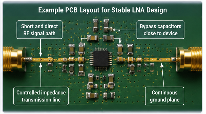
PCB layout significantly impacts LNA stability. Many oscillation problems that appear to be circuit issues are actually layout problems that can be solved without changing the schematic.
Critical Layout Rules
Ground and Decoupling
- Use solid, continuous ground planes beneath all RF traces
- Place vias within 0.5mm of all ground connections
- Use multiple small vias (0.3-0.5mm) rather than single large vias
- Implement star grounding for bias circuits
- Separate analog and digital grounds
- Provide adequate decoupling at device pins
Input/Output Isolation
| Layout Issue | Problem | Solution |
|---|---|---|
| Long Input Trace | Radiation, coupling | Keep traces short, use guard rings |
| Parallel I/O | Feedback coupling | Maximize separation distance |
| Ground Slots | Slotline modes | Fill slots, use solid planes |
| Via Stubs | Resonance | Use blind/buried vias or antipads |
Decoupling Network Layout
Proper decoupling is essential to prevent power supply feedback:
Decoupling Best Practices
- Place decoupling capacitors within 2mm of device pins
- Use multiple capacitor values (100pF + 1nF + 10uF)
- Route bias lines with wide traces or dedicated planes
- Use chip capacitors with minimal lead inductance
- Consider ferrite beads for additional RF isolation
Measurement and Verification
Proper measurement techniques ensure that stabilization measures are effective and the LNA remains stable under all operating conditions.
Stability Measurement Setup
- Connect VNA: Measure S-parameters from 100 MHz to 3x operating frequency
- Calculate Stability: Verify K > 1 and Mu > 1 across entire range
- Check Delta: Plot stability circle delta for potential instability regions
- Measure with Bias: Test at minimum, typical, and maximum bias conditions
- Temperature Sweep: Verify stability from min to max operating temperature
Detecting Potential Oscillation
Warning Signs in S-Parameters
- |S11| or |S22| approaching or exceeding unity (potential instability)
- Negative resistance regions (real part of Zin < 0)
- K < 1 at any frequency within or near operating band
- Mu < 1 indicating potential instability
- Sharp resonances in S-parameter plots
Output Spectrum Test
Even with good S-parameters, hidden oscillations can exist:
- Terminate input with 50 ohms, observe output spectrum
- Look for spurious signals above noise floor
- Test with and without input signal applied
- Use close-in RBW to detect low-level oscillations
- Check across full temperature and bias range
Final Verification Checklist
- Stability factor K > 1.5 across full frequency range
- Mu > 1.2 minimum stability margin
- No spurious signals in output spectrum
- Stable under all bias conditions
- Stable across full temperature range
- Stable with various source/load impedances
- No oscillation during power-up/power-down transients
Frequently Asked Questions
Conclusion
Eliminating oscillation in Low Noise Amplifiers requires a systematic approach combining stability analysis, careful design, proper layout, and thorough measurement. Understanding the mechanisms that cause oscillation enables engineers to implement effective stabilization techniques while minimizing performance degradation.
The key to success is designing for stability from the beginning rather than treating oscillation as an afterthought. Use stability analysis tools during simulation, implement proper layout practices, and verify stability across all operating conditions before proceeding to production.
When oscillations do occur, follow the diagnostic process: identify the oscillation frequency and type, determine the root cause, implement appropriate stabilization techniques, and verify effectiveness through comprehensive testing. With proper attention to stability throughout the design process, reliable oscillation-free LNA operation can be consistently achieved.
Need Help with Your LNA Design?
Our RF engineering team can help diagnose oscillation issues and implement effective stabilization solutions for your LNA applications.
Contact Our Technical Team