

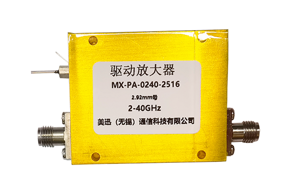



Understand what a bias tee is, how it works, its key functions, electrical characteristics, and applications in RF, microwave, wireless, and high-frequency testing systems.
Sep 02 ,26


5G communication testing, wireless terminal automated testing
Aerospace communication systems
Precision measurement equipment, radio frequency signal control of radar transmitters
Communication and navigation systems
Optical communication module-related testing
Interconnection of wireless communication base stations
A comprehensive technical exploration of DC-RF isolation fundamentals, its impact on microwave system performance, and actionable design strategies for achieving superior isolation in bias tee circuits.
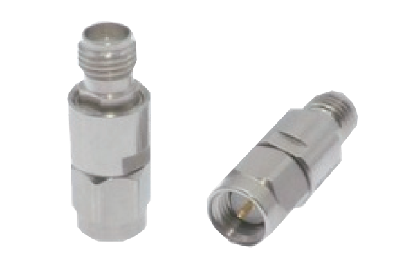
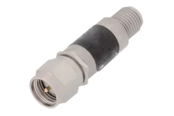
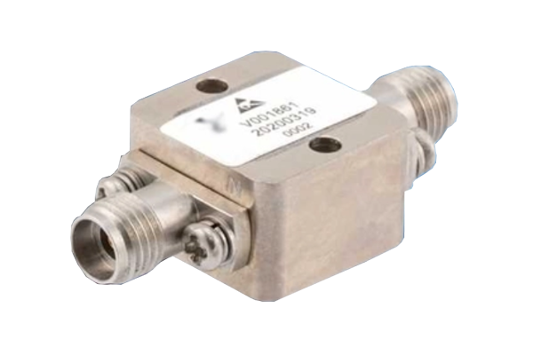
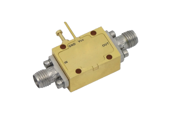
In the realm of microwave and RF circuit design, the bias tee stands as one of the most fundamental yet frequently misunderstood components. At its core, a bias tee is a three-port network that combines or separates DC bias signals from high-frequency RF signals. The effectiveness of this separation is quantified by a parameter known as DC-RF isolation — and it is this very parameter that often determines whether a microwave system performs flawlessly or fails catastrophically.
DC-RF isolation refers to the degree of attenuation experienced by an RF signal as it attempts to traverse the DC path of a bias tee, and conversely, the level of DC leakage that appears on the RF port. In an ideal bias tee, the DC port would present an infinite impedance to RF signals while the RF port would be completely transparent to them. In reality, every component introduces parasitic elements that compromise this ideal behavior.
DC-RF isolation is typically expressed in decibels (dB) and is defined as the ratio of RF power incident on the DC port to the RF power delivered to the RF port. A bias tee with 40 dB of isolation means that only 0.01% of the RF energy leaks into the DC path — a standard benchmark for high-performance designs.
The importance of high DC-RF isolation extends far beyond a simple specification on a datasheet. Poor isolation can introduce a cascade of performance issues that ripple through the entire microwave signal chain. Below are the critical reasons why engineers must prioritize isolation in their bias tee designs.
When RF energy leaks into the DC path, it travels directly toward the power supply or bias circuitry. Modern switching power supplies and linear regulators are not designed to handle high-frequency signals superimposed on their output rails. This unwanted RF contamination can cause:
The converse problem — DC leakage into the RF path — is equally damaging. When DC bias voltage bleeds onto the RF port, it can saturate sensitive receiver front-ends, distort transmitted waveforms, and introduce unwanted spectral components. A mere 50 mV of DC offset on a high-speed data line can shift the eye diagram enough to increase bit error rates dramatically.
Low isolation often correlates with higher intermodulation distortion (IMD) products. When RF energy penetrates the DC bias network, it can mix with other signals present in the bias circuitry, generating spurious harmonics and intermodulation products that degrade the system's dynamic range. This is particularly critical in multi-carrier communication systems where third-order intercept point (IP3) is a key performance metric.
To understand how isolation is achieved and where it breaks down, one must examine the two primary building blocks of a bias tee: the DC blocking capacitor and the RF choke inductor.
| Component | Primary Function | Isolation Contribution | Typical Isolation Level | Failure Mode |
|---|---|---|---|---|
| DC Blocking Capacitor | Passes RF signal while blocking DC voltage | Prevents DC from reaching RF port | 40–60 dB | Capacitor resonance, voltage breakdown |
| RF Choke Inductor | Passes DC bias while blocking RF signal | Prevents RF from reaching DC port | 30–50 dB | Self-resonance, saturation |
| Transmission Line Structure | Maintains 50Ω characteristic impedance | Minimizes reflections and mode conversion | > 50 dB | Impedance discontinuities, crosstalk |
| Ground Plane Integrity | Provides return path and shielding | Suppresses parasitic coupling paths | 20–40 dB | Slot resonances, ground bounce |
The self-resonant frequency (SRF) of the choke inductor is the single most critical parasitic parameter. Below the SRF, the inductor behaves as expected, providing increasing impedance with frequency. Above the SRF, however, the inductor's parasitic capacitance dominates, causing the impedance to decrease — effectively destroying isolation at higher frequencies. This is why wideband bias tees often employ multiple cascaded inductors with staggered self-resonant frequencies to extend the usable bandwidth.
Achieving high DC-RF isolation is not a matter of simply selecting the right inductor and capacitor. It demands a holistic approach that considers the entire electromagnetic environment. Below are the essential design practices that distinguish high-performance bias tees from mediocre ones.
Accurate measurement of DC-RF isolation requires careful attention to test setup. A vector network analyzer (VNA) is the primary instrument, configured to measure S21 between the DC port and the RF port. The test should be performed with the unused port terminated in the appropriate impedance (usually 50Ω) to simulate real operating conditions.
Key parameters to verify include:
High DC-RF isolation is not merely a desirable characteristic in microwave bias tee design — it is an essential requirement for reliable system operation. Engineers who prioritize isolation from the outset of the design process, paying meticulous attention to component selection, layout geometry, and parasitic management, will consistently achieve superior performance. Those who treat isolation as an afterthought will inevitably face mysterious oscillations, degraded signal quality, and field failures that are notoriously difficult to diagnose.
The bias tee may appear simple in concept, but its design embodies a delicate balance between DC handling capability, RF transparency, and isolation performance. As microwave systems push toward higher frequencies, wider bandwidths, and greater integration density, the demand for high DC-RF isolation becomes increasingly stringent.
Whether you are designing a bias tee for a satellite communication transceiver, a radar system, a laboratory test setup, or a 5G base station, understanding and optimizing DC-RF isolation will directly impact the success of your design. By applying the principles and practices outlined in this article — careful component selection, strategic layout, rigorous measurement, and iterative optimization — you can ensure that your bias tee delivers the isolation performance your application demands.
Remember: in the world of microwave engineering, what you cannot isolate will inevitably find a way to compromise your system.
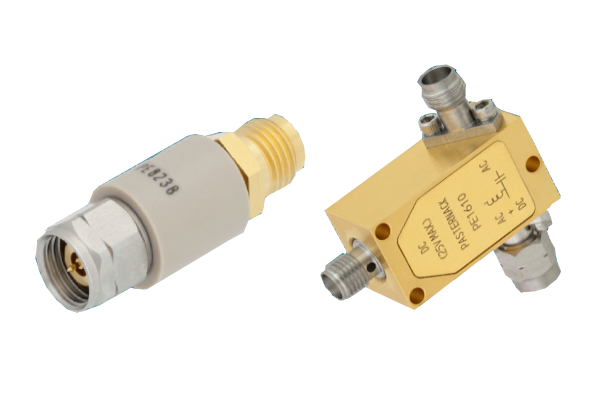
High-tech Enterprise, Feifeng Talent
Chief Engineer Wang graduated with a master's degree in high-power microwave from the Institute of Electronics, University of Chinese Academy of Sciences.
View Full Profile