






RF Amplifier Circuit: Design, Topologies & Best Practices
Quick Answer
An RF amplifier circuit uses a transistor (BJT, FET, GaN, LDMOS, GaAs) biased at a chosen operating point, with input/output matching networks to transform between 50 Ω and the device's optimal impedance. Classes A through F set the trade-off between linearity and efficiency. Successful designs combine careful DC bias, broadband matching, stable layout, and proper thermal management.
What Is an RF Amplifier Circuit?
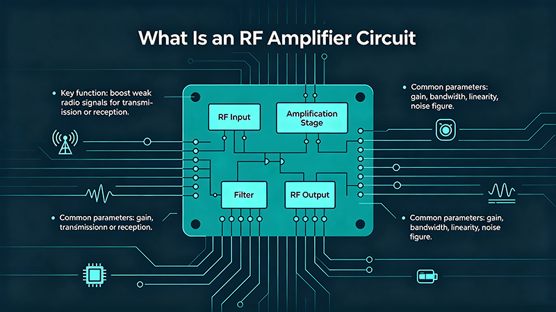
An RF amplifier circuit is an electronic circuit that increases the power of an RF signal while preserving its information content. It typically contains:
- Active device: transistor that provides gain (BJT, JFET, MOSFET, GaN HEMT, GaAs pHEMT).
- DC bias network: sets the quiescent operating point (Q-point) and supplies stable DC.
- Input matching network: transforms 50 Ω to the source impedance that delivers maximum gain or lowest noise.
- Output matching network: transforms the device's load-line impedance to 50 Ω.
- Stability network: prevents unwanted oscillations at any frequency.
- RF choke and DC blocking: isolates DC from RF paths and vice from.
How an RF Amplifier Circuit Works
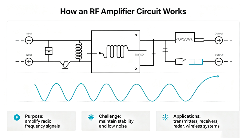
Generic RF Amplifier Block Diagram
The RF signal enters the input match, is amplified by the transistor, and exits through the output match. Bias is supplied via chokes that look open at RF but short at DC.
Amplifier Operating Classes
| Class | Conduction Angle | Efficiency | Linearity | Typical Use |
|---|---|---|---|---|
| A | 360° | ≤ 50 % | Excellent | Low-noise receivers, drivers |
| AB | 180° – 360° | 50 – 70 % | Good | Cellular, broadcast |
| B | 180° | ≤ 78.5 % | Moderate | Push-pull audio, RF |
| C | < 180° | ≤ 100 % (theoretical) | Poor (constant envelope only) | FM, CW transmitters |
| F / Inverse F | Harmonic-tuned | > 90 % | Narrowband | High-power pulsed RF |
| Doherty | Carrier + Peaking | 40 – 50 % at 8 dB back-off | Good | Cellular base stations |
Common RF Amplifier Topologies
Common-Source (FET) / Common-Emitter (BJT)
Single-transistor amplifier with grounded source/emitter. Simplest, but lowest gain and only moderate bandwidth.
Cascode Amplifier
Two stacked transistors: one as common-source, one as common-gate. Higher gain, better isolation, wider bandwidth.
Differential Pair
Two transistors sharing a tail current. Rejects common-mode noise, drives balanced loads, used in mixers and op-amp RF front-ends.
Push-Pull Amplifier
Two transistors operating in anti-phase. Cancels even-order harmonics, doubles output swing, improves efficiency.
Doherty Amplifier
Carrier + peaking amplifier with a quarter-wave combiner. High efficiency at backed-off power; standard for OFDM base stations.
Balanced Amplifier
Two amplifiers combined with 90° hybrids. Improved VSWR, twice the power, but 3 dB extra loss from the hybrids.
Distributed Amplifier
Multiple transistors with transmission-line gate/drain connections. Ultra-wide bandwidth from DC to tens of GHz.
Feedback Amplifier
Resistor or transformer feedback trades gain for flat bandwidth and stable 50 Ω match. Common in MMIC design.
Key Components
| Component | Function |
|---|---|
| Transistor | Provides gain |
| Bias resistors / current source | Set quiescent operating point |
| RF choke (inductor) | Feeds DC, blocks RF |
| DC blocking capacitor | Passes RF, blocks DC |
| Matching network (L/C) | Transforms impedance |
| Stability resistor / ferrite bead | Suppresses low-frequency oscillation |
| Decoupling capacitors | Short RF to ground on supply rails |
| Heatsink / thermal via | Removes heat from the transistor |
Design Steps
1. Define Specs
Frequency, bandwidth, gain, P1dB, IP3, NF, VSWR, supply voltage.
2. Choose Device
Select transistor technology and package based on power, frequency, noise, and cost.
3. Bias Point
Set Q-point from device curves. Add active bias to stabilize against temperature.
4. Matching
Design input/output match for gain, NF, or power, depending on stage role.
5. Stability
Check Rollett's condition over frequency; add resistive loading if needed.
6. Layout
Use controlled-impedance traces, short ground paths, and proper component placement.
7. Simulate
Use SPICE, Microwave Office, or ADS with device models and S-parameter data.
8. Build & Test
Prototype, measure S-parameters, gain, P1dB, NF; iterate as needed.
PCB Layout Best Practices
- Use a continuous ground plane on the layer closest to RF traces.
- Keep RF traces short and impedance-controlled (50 Ω typical).
- Place decoupling capacitors within 1 – 2 mm of supply pins.
- Use via stitching to suppress parallel-plate modes.
- Keep input and output traces physically separated to prevent feedback.
- Use thermal vias under the transistor to conduct heat to inner layers or the back side.
- Avoid 90° trace bends; use 45° or curved traces.
Common Mistakes
- Missing DC blocking: DC on RF ports can damage the next stage.
- Poor grounding: long ground paths create parasitic inductance and instability.
- Unstable bias: passive bias resistors drift with temperature; use active bias or.
- Insufficient decoupling: supply-line resonances cause oscillation.
- Ignoring stability: an amplifier that oscillates at low power delivers no useful signal.
- Wrong load line: the output match sets the operating point; mismatched loads destroy devices.
Verification & Measurement
- Measure S-parameters with a calibrated VNA; check gain, return loss, isolation.
- Measure P1dB with a swept source and power meter.
- Measure two-tone IP3 with two closely-spaced CW tones.
- Measure noise figure with a noise source and NF analyzer.
- Test stability by varying load VSWR and source impedance.
- Thermal-test under CW drive to verify heatsink sizing.
Real-World Applications
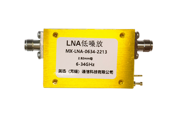
- Low-noise amplifiers (LNAs): satellite receivers, GPS, cellular base stations.
- Driver amplifiers: feed power stages from small-signal sources.
- Power amplifiers: Wi-Fi, cellular, radar, broadcast.
- Broadband amplifiers: oscilloscopes, spectrum analyzers, instrumentation.
- Cable TV distribution: push-pull and power-doubler amplifier modules.
- Radar T/R modules: integrated GaN amplifier circuits with switching.
Key Takeaways
- An RF amplifier circuit uses a transistor, bias, and matching networks.
- Operating class determines the linearity / efficiency trade-off.
- Cascode, push-pull, Doherty, and balanced topologies solve particular problems.
- Stability analysis is mandatory — never ship an unverified amplifier.
- PCB layout, grounding, and thermal management are as critical as the schematic.
Frequently Asked Questions
What is an RF amplifier circuit?
An RF amplifier circuit uses a transistor to amplify radio-frequency signals. It consists of a transistor, DC bias network, input and output matching, and stability networks.
Which operating class should I use?
Use Class A for low-noise amplifiers where linearity matters most. Use Class AB for cellular and broadcast where efficiency and linearity must balance. Use Doherty for high-efficiency cellular base stations.
What is unconditional stability?
An amplifier is unconditionally stable if it does not oscillate for any passive source and load impedance. Check Rollett's condition (|Δ| < 1 and K > 1) before shipping a design.
How do I match 50 Ω to a transistor?
Use an L-network, π-network, or T-network of lumped inductors and capacitors. For microwave frequencies, use microstrip or stripline segments. Optimize with Smith-chart tools or ADS.
What is the difference between gain and PAE?
Gain is the ratio of output power to input power, measured in dB. PAE (Power-Added Efficiency) is (Pout − Pin) / PDC, describing how efficiently DC power becomes useful RF.
About the Author — MeiXun Team
Chief Engineer Wang
High-tech Enterprise, Feifeng Talent
Chief Engineer Wang graduated with a master's degree in high-power microwave from the Institute of Electronics, University of Chinese Academy of Sciences.
View Full Profile- RF Switch Circuit Diagram
- RF Switch
- Ohm's Law
- dBm to Watt
- mW to dBm
- Wavelength to Frequency
- RF Connector
- SMA Connector
- RF Switch Module
- RF Coupler
- RF PIN Switch
- Microwave Coaxial Switch
- PIN Switch
- Coaxial RF Switch
- Waveguide Switch
- Microwave Switch
- Low Noise Amplifier
- PIN Diode Switch
- Coaxial Switch
- RF Microwave Switch
- SPST Switch