

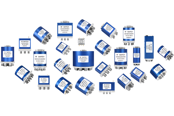


Response Time of PIN Diode Switches
The response time of a PIN diode switch determines how quickly it can transition between ON (low impedance) and OFF (high impedance) states, which is critical in RF, microwave, and high-speed switching applications.
1. Typical Response Time Range
-
Turn-on time (forward bias): 1–100 ns (depends on diode structure & drive current).
-
Turn-off time (reverse bias): 10–1000 ns (limited by carrier recombination in the intrinsic "I" layer).
2. Key Factors Affecting Speed
-
I-layer thickness: Thinner layers (~10–100 µm) enable faster switching but reduce power handling.
-
Bias current: Higher forward current (e.g., 10–100 mA) speeds up turn-on.
-
Reverse bias voltage: Stronger reverse bias (e.g., −5V to −50V) accelerates carrier sweep-out, reducing turn-off time.
-
Circuit design: Low-inductance drivers minimize delay.
3. Comparison with Other Switches
-
Faster than mechanical/relay switches (ms range) but slower than GaAs FETs (sub-ns).
-
Preferred for medium-speed RF switching (e.g., T/R modules, antenna tuning).
4. Measurement Methods
-
Pulse testing: Apply square-wave bias and measure rise/fall with an oscilloscope.
-
Network analyzers: Evaluate settling time in RF systems.
Applications:
-
Radar systems: Fast switching for pulse modulation.
-
5G/6G networks: Beamforming and frequency hopping.