

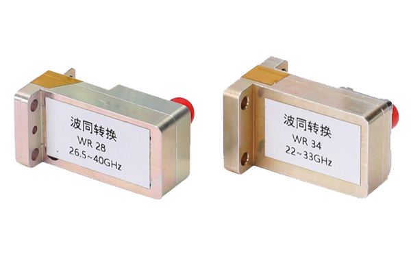


How to solve signal interference issues in waveguide switches
Addressing Signal Interference in Waveguide Switches
A systematic approach focusing on design optimization, material selection, environmental control, and assembly precision is essential for mitigating signal interference issues in waveguide switches.
Design Optimization
- Refine internal cavity design for smooth signal propagation paths
- Minimize sharp edges or abrupt changes that cause signal reflection
- Use curved or gradual transitions to reduce impedance mismatches
- Implement physical barriers or segmented chambers to prevent cross-coupling
Material Selection
- Use high-conductivity metals (copper/aluminum with silver/gold plating)
- Choose dielectric materials with low dielectric loss and stable electrical properties
- Incorporate electromagnetic shielding materials around the switch housing
- Avoid poor-quality dielectrics that can introduce signal distortion
Environmental Control
- Maintain stable temperature and low humidity conditions
- Position away from high-power electromagnetic sources
- Monitor and control operating environment to prevent impedance shifts
- Protect against external electromagnetic radiation
Assembly Precision
- Ensure tight, secure connections at flange interfaces
- Use gaskets or sealing materials at connection points
- Implement proper grounding of switch housing and internal components
- Eliminate gaps that can leak signals or allow external interference
Impedance Matching
- Integrate impedance matching networks into switch design
- Align switch impedance with connected waveguide system
- Reduce signal reflection at interfaces
- Ensure efficient signal transfer throughout the system
By combining these strategies—structural optimization, careful material choice, environmental control, precise assembly, and impedance matching—signal interference in waveguide switches can be effectively minimized, ensuring reliable and consistent performance.