


How to Reduce the Noise Figure of an RF Low-Noise Amplifier
RF Low-Noise Amplifier Optimization
Key strategies for reducing noise figure in RF amplifier design
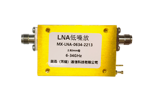
Device Selection & Parameter Matching
- The key to reducing the noise figure begins with device selection. Semiconductor materials and transistors with low noise figures should be prioritized.
- Device parameters should be matched according to the operating frequency band and application scenario.
- By selecting the appropriate device model, noise generation can be reduced at the source, laying the foundation for a low-noise RF amplifier.
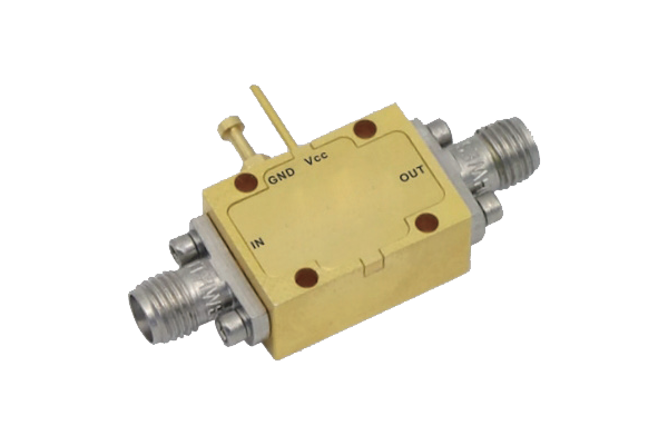
Circuit Design & Layout Optimization
- The input matching network must be precisely designed to achieve optimal matching between the signal source and the amplifier's input impedance.
- The bias design must provide a stable operating point to avoid increased noise due to current or voltage fluctuations.
- The layout should shorten high-frequency signal lines and reduce parasitic inductance and capacitance.
Operating Environment & Conditions Control
- A stable operating environment is crucial. Extreme temperature fluctuations must be avoided.
- External electromagnetic interference should be reduced using shielding or isolation.
- Ensure that the power supply is stable and pure to prevent power supply noise from entering the amplifier unit.
System-Level Co-design & Debugging
- The RF low-noise amplifier must be optimized in conjunction with the front-end components.
- The front-end filter should be low-insertion-loss to minimize signal attenuation.
- During debugging, we need to fine-tune the impedance matching network to ensure optimal noise matching.