

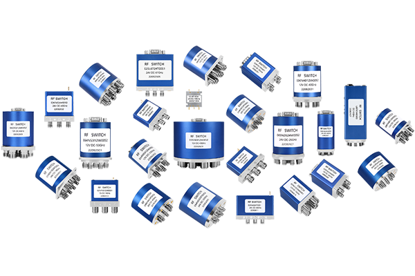


How to reduce the insertion loss of coaxial switch
Technical Approaches to Reduce Coaxial Switch Insertion Loss
1. Optimizing Contact Design
- Material Selection: Use gold-plated beryllium copper/tungsten-copper for high conductivity.
- Contact Mechanics: Ensure precise alignment, sufficient pressure, and self-cleaning (e.g., wiping action) for low resistance.
2. Material Selection for Signal Paths
- Dielectrics: Use low-loss PTFE/air (air-dielectric for high RF performance).
- Conductors: Oxygen-free copper with smooth inner surfaces; avoid magnetic materials.
3. Structural Symmetry & Impedance Matching
- Geometry: Maintain strict 50Ω symmetry; use tapered/stepped transitions for minimal reflections.
- Simulation: HFSS optimization for S11 < -20dB across the signal path.
4. Thermal Management
- Heat Dissipation: Integrate heat sinks/thermal vias for high-power switches (>100W).
- Thermal Materials: Graphite pads for uniform heat distribution and anti-overheating.
5. Manufacturing Precision & Surface Finish
- Surface Treatment: Electroless nickel + gold plating (Ra < 0.2μm) for smooth inner conductors.
- Machining Tolerance: ±5μm precision for gaps/spacing to minimize mechanical variations.
6. Frequency Band Design
- Narrowband Optimization: Resonant structures (e.g., quarter-wave stubs) for specific frequencies.
- Multi-Band Solutions: Switched filter banks/modular designs for tailored impedance matching.