

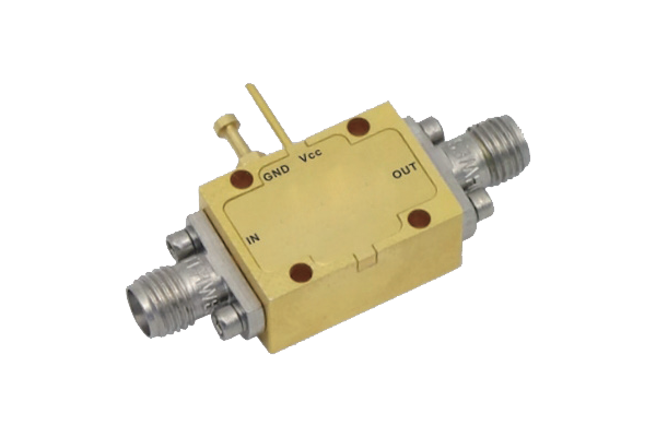
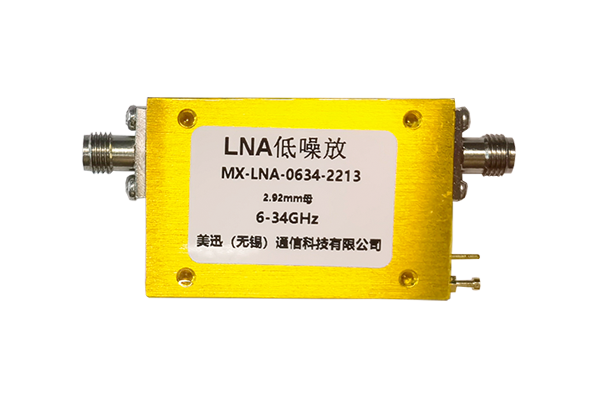


How to Optimize LNA Amplifier Gain
LNA Amplifier Design Guidelines
Key considerations for optimizing Low Noise Amplifier performance in RF applications
1
Optimizing Circuit Matching
- Design input/output matching networks based on operating frequency band
- Minimize reflection losses during signal transmission
- Select matching component parameters carefully
- Ensure efficient signal energy transfer to LNA amplifier core
- Minimize gain attenuation from impedance mismatch
2
Device Selection
- Select transistors or ICs with high gain characteristics
- Consider inherent amplification capabilities
- Pay attention to device frequency response characteristics
- Ensure stable gain output within target operating frequency band
- Avoid limitations from inherent device performance deficiencies
3
Properly Designing Bias Circuit
- Provide stable operating point for core device
- Prevent gain drift from voltage/current fluctuations
- Optimize bias network parameters
- Ensure device operates at optimal amplification state
- Minimize impact of environmental changes on gain
4
Balancing Noise and Gain
- Avoid excessively pursuing high gain at expense of noise figure
- Optimize circuit topology for both gain and low noise
- Effectively amplify weak signals while maintaining signal quality
- Consider trade-offs between gain and noise performance
5
Focus on Heat Dissipation Design
- Address heat generated during operation
- Prevent performance degradation from temperature effects
- Design proper heat dissipation structure
- Ensure device operates at appropriate temperature
- Avoid gain degradation from overheating