


How to Optimize Impedance Matching in Coaxial Switches
Coaxial Switch Impedance Matching Optimization
Impedance matching is critical for minimizing signal reflection and ensuring maximum power transfer in coaxial switches. Poor matching can lead to insertion loss, VSWR degradation, and signal distortion, especially in high-frequency applications (e.g., 5G, radar, RF testing). Below are key optimization strategies:
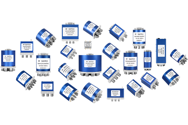
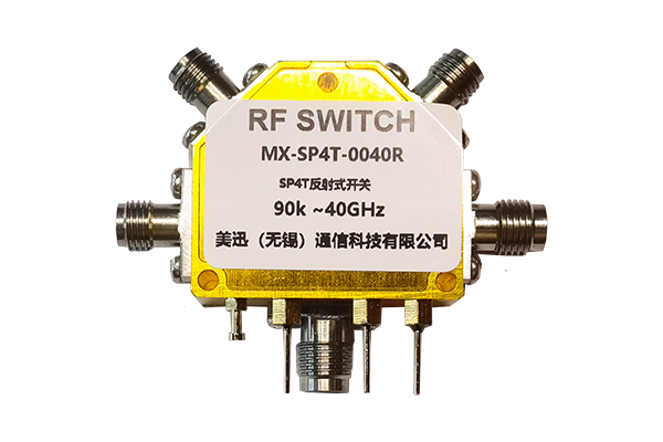
1. Select the Right Switch for Target Frequency
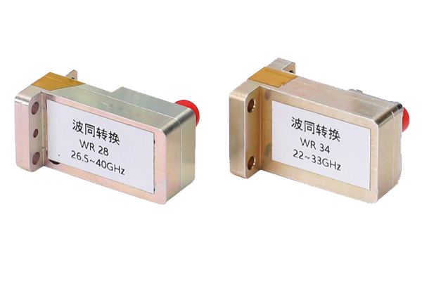
- Ensure the coaxial switch’s characteristic impedance (typically 50Ω or 75Ω) matches the system.
- Verify the frequency range (e.g., DC-18 GHz) and VSWR specs (e.g., <1.5:1) for your application.
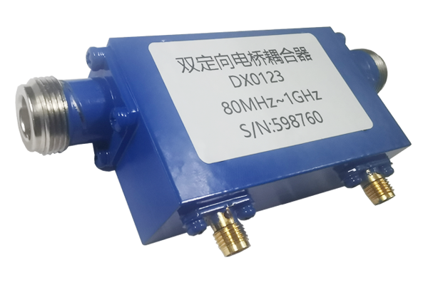
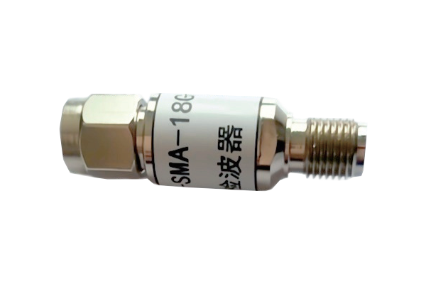
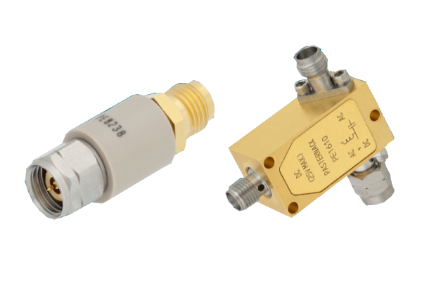
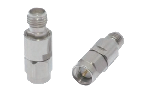
2. Minimize Connector and Interface Mismatches
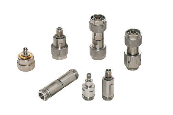
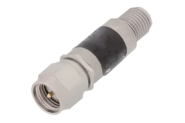
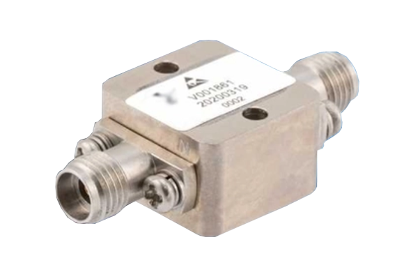
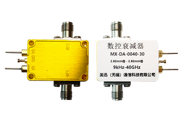
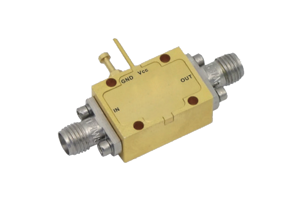
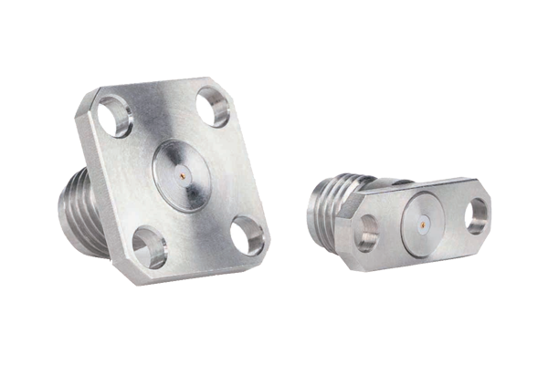
- Use high-quality connectors (SMA, N-type, 2.92mm) with consistent impedance.
- Avoid adapters; direct connections reduce discontinuities.
- Torque connectors to manufacturer specs to ensure proper contact.
3. Optimize PCB/Transmission Line Transitions
- For PCB-mounted switches, use controlled-impedance traces with minimal bends.
- Implement ground vias near transitions to reduce parasitic inductance/capacitance.
4. Mitigate Internal Reflections
- Choose switches with low return loss (e.g., >20 dB).
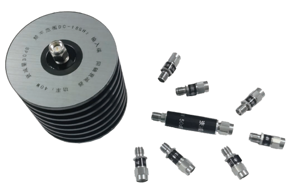
- For multi-port switches, terminate unused ports with 50Ω loads to prevent reflections.
5. Calibration and Testing
- Use a vector network analyzer (VNA) to measure S11 (reflection) and S21 (insertion loss).
- Apply time-domain reflectometry (TDR) to locate impedance mismatches.
Advanced Techniques
- Tuning elements (stubs, capacitors) can compensate for minor mismatches.
- Electromagnetic simulation (e.g., HFSS) helps model and optimize layouts.