

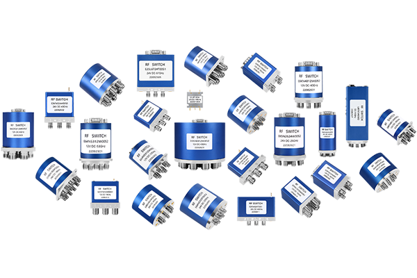
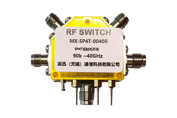


How to Improve the Isolation of an RF Pin Diode Switch
RF Pin Diode Switch Optimization Guide
Effective strategies to enhance performance and isolation of RF pin diode switches
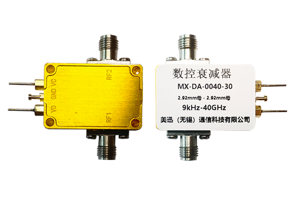
Optimize Circuit Topology Design
- Use multi-stage diode configurations: Multi-stage series or parallel diode combinations can be used to enhance signal blocking capabilities through the synergistic effect of multiple diodes, avoiding insufficient isolation due to the performance limitations of a single diode.
- Implement precise impedance matching: Accurately matching the impedance parameters in the circuit ensures reduced signal reflection and leakage during transmission.
- Add impedance matching networks: Further stabilizes the forward conduction and reverse cutoff states of the diodes, reducing crosstalk from non-target signals and strengthening isolation at the circuit architecture level.
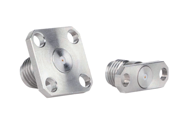
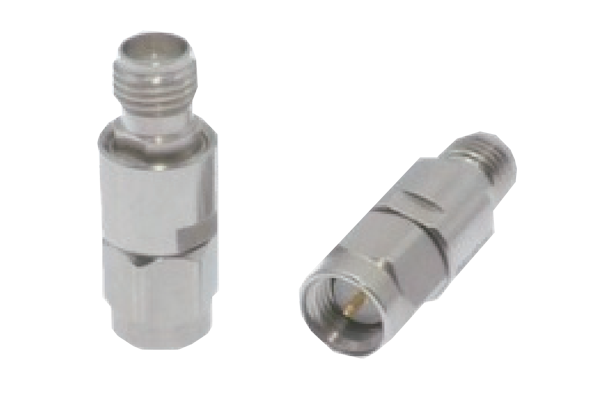
Strictly Control Component Selection
- Prioritize diodes with optimal parameters: Select RF pin diode switches with high reverse breakdown voltage and low reverse leakage current to more effectively block signal penetration in the cutoff state.
- Minimize parasitic parameters: Choose diodes with low parasitic parameters to reduce the impact of their inter-electrode capacitance and series resistance on high-frequency signals.
- Use high-performance peripheral components: Select low-loss inductors and capacitors to ensure the signal isolation capability of the entire switching circuit is not affected by external component performance.
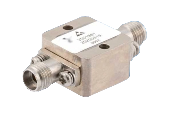
Improve PCB Structure Layout
- Separate input and output ports: Keep the input and output ports of the switching circuit apart to avoid direct signal coupling caused by excessively close wiring.
- Optimize ground plane design: Increase the area of the ground plane to ensure a short and wide ground path, reducing ground impedance and minimizing crosstalk.
- Strategic component placement: Rationally plan the diode mounting positions to avoid diodes being too close to other high-frequency components.
- Implement shielding measures: Use metal shielding covers for critical signal paths to block external interference and prevent signal leakage within the RF pin diode switch.
Suppress Signal Interference Sources
- Install filter networks: Place filter networks around the switching circuit to filter out external noise signals and prevent them from affecting isolation performance.
- Separate control and RF signals: Optimize wiring by separating control signals from RF signals to prevent interference from control signals affecting RF performance.
- Use shielded wiring: Implement shielded wiring for control signal transmission to further reduce interference intensity.
- Stabilize power supply: Ensure power supply stability by adding power supply filter capacitors to reduce the impact of power supply noise on the diode's operating state.