

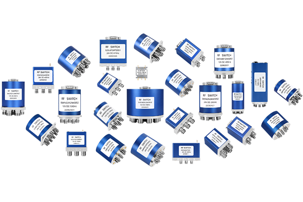


How to Control Signal Loss in Coaxial Switches
Signal loss is a critical concern in coaxial switches, as it directly impacts the integrity of RF/microwave signals in communication, radar, and testing systems. Controlling this loss requires meticulous design, material selection, and manufacturing precision. Below are key strategies to minimize signal loss and optimize performance:
1. Material Selection for Low Loss
The choice of materials in connectors, contacts, and transmission paths is fundamental:
- Conductor Materials: High-conductivity metals like oxygen-free copper (OFC) or gold-plated surfaces reduce ohmic losses. Gold plating also enhances corrosion resistance and maintains low contact resistance over time.
- Dielectric Materials: Low-loss dielectrics (e.g., PTFE, ceramic, or air) between conductors minimize energy dissipation. For example, air-filled coaxial structures offer the lowest dielectric loss but require robust mechanical designs to prevent signal leakage.
- Contact Materials: Precious metals (gold, silver) or advanced alloys (e.g., beryllium copper with gold plating) ensure low contact resistance and stable conductivity during switching.
2. Precision Mechanical Design
Mechanical tolerances directly affect signal propagation:
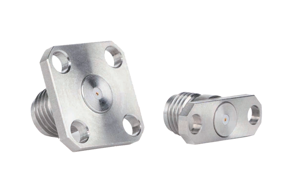
- Impedance Matching: The switch’s internal structure must maintain a consistent 50Ω (or other specified) impedance to avoid reflections. This requires precise control of conductor diameters, dielectric thickness, and contact alignment.
-
Contact Geometry:
- Spring-Loaded Contacts: Ensure reliable, low-force connections to reduce deformation and oxidation while maintaining consistent contact area.
- Smooth Transitions: Rounded edges and gradual transitions between sections (e.g., from the switch blade to the coaxial line) minimize electromagnetic field discontinuities and scattering losses.
- Hermetic Sealing: Sealed designs prevent moisture, dust, or gas intrusion, which can degrade dielectric performance and increase loss over time.
3. Manufacturing and Assembly Techniques
High-precision fabrication processes are essential:
- CNC Machining: Tight tolerances in connector and housing fabrication (e.g., ±0.001 mm) ensure consistent impedance and minimal signal reflections.
- Plating Uniformity: Even, thin gold or nickel plating (e.g., 2–5 μm thickness) on contact surfaces reduces oxidation and maintains low contact resistance without adding excessive material that could alter impedance.
- Alignment and Calibration: Post-assembly, switches undergo rigorous testing (e.g., vector network analysis) to measure insertion loss, VSWR, and phase stability. Adjustments may include re-tuning contacts or replacing misaligned components.
4. Thermal Management
Heat generated during high-power operation can degrade materials and increase loss:
- Heat Dissipation Design: Metal housings (e.g., aluminum or copper) with heat sinks or thermal interface materials conduct heat away from high-power sections, preventing dielectric breakdown or contact deformation.
- Temperature Rating: Select switches with wide operating temperature ranges (e.g., -40°C to +85°C) to maintain material stability and contact integrity across environments.
5. Switching Mechanism Optimization
The type of switching mechanism affects both loss and reliability:
-
Electromechanical Switches (EMS):
- Use low-force actuators to minimize contact wear while ensuring firm connections.
- Magnetic latching designs reduce power consumption and heat generation during static operation.
-
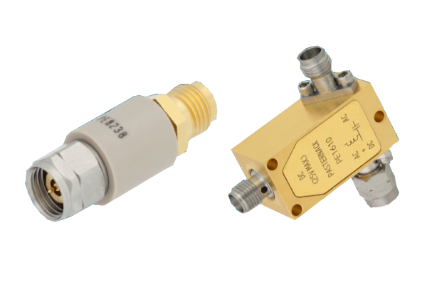
Solid-State Switches (SSS):
- Semiconductor-based switches (e.g., PIN diodes, FETs) have no moving parts, reducing mechanical wear but may introduce insertion loss due to parasitic capacitances/inductances.
- Advanced topologies (e.g., balanced designs, distributed amplifiers) can compensate for semiconductor losses at higher frequencies.
6. Environmental and Operational Considerations
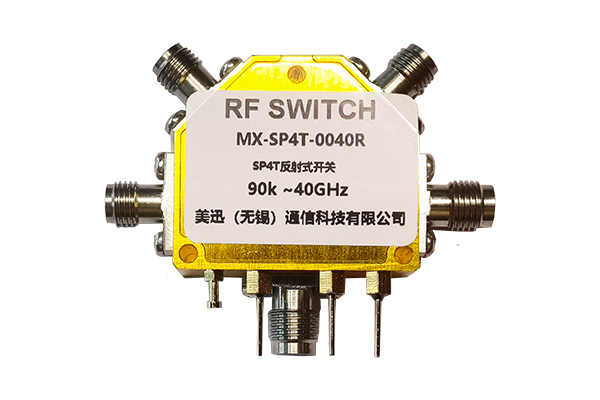
- Frequency Range: Choose switches rated for the target frequency band (e.g., DC to 40 GHz) to avoid out-of-band losses from inadequate bandwidth.
- Power Handling: Match the switch’s power rating to the system’s peak and average power to prevent arcing or thermal damage, which increase loss.
- Maintenance Practices: Regular cleaning of contacts (e.g., with non-abrasive solvents) and inspection for wear (e.g., pitting, oxidation) can restore low-loss performance in mechanical switches.
7. Testing and Validation
- Vector Network Analyzer (VNA): Measures insertion loss, return loss, and phase shift across the frequency range to identify problematic bands.
- Life Cycle Testing: Simulate millions of switch cycles to ensure contact resistance remains stable and mechanical components do not degrade into high-loss states.
- Environmental Testing: Subject switches to humidity, vibration, or temperature cycles to verify that sealing and material stability prevent loss variations.