

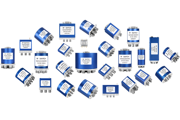


How to avoid coaxial switch signal reflection problem
To avoid signal reflection issues in coaxial switches, proper design, installation, and maintenance are critical. Signal reflections occur when impedance mismatches exist between the switch, cables, and connected components, causing part of the signal to bounce back rather than propagate forward. Here’s a detailed guide to mitigating these issues:
1. Ensure Impedance Matching
The primary cause of reflections is impedance mismatches. Coaxial systems typically use 50 Ω or 75 Ω standards.
- Component Selection: Use coaxial switches, cables, connectors, and devices (e.g., amplifiers, antennas) with matched impedance ratings. For example, a 50 Ω switch must connect to 50 Ω cables and loads.
- Design Tolerances: Manufacturers should optimize switch internals (e.g., contact gaps, center conductor geometry) to maintain consistent impedance through signal paths. Even minor dimensional variations can create mismatches at high frequencies.
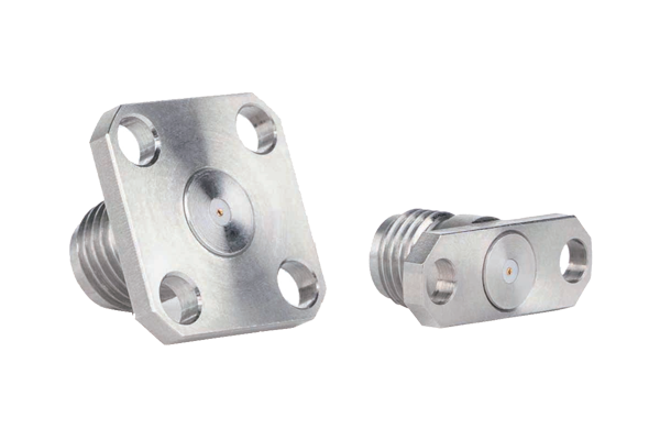
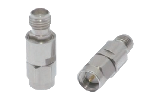
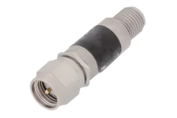
2. Use High-Quality Connectors and Cables
Loose, corroded, or poorly terminated connectors are major sources of reflections.
- Secure Terminations: Ensure connectors are tightly crimped, soldered, or clamped to cables to avoid mechanical gaps. For field installations, use torque wrenches to achieve standardized tightness.
- Cable Integrity: Avoid kinking, bending, or over-stretching coaxial cables, as this deforms the dielectric and conductor, altering impedance. Follow minimum bend radius specifications (typically 5–10× the cable diameter).
- Material Quality: Choose low-loss cables with robust shields (e.g., braided copper or aluminum) to prevent moisture ingress or oxidation, which degrade conductivity and impedance stability.
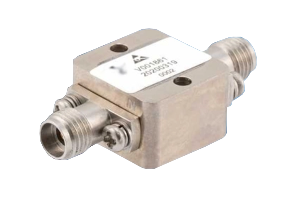
3. Optimize Switch Design for Low VSWR
Voltage Standing Wave Ratio (VSWR) is a key metric for reflections. A VSWR of 1:1 indicates perfect matching; higher values (e.g., 1.5:1) signal mismatches.
- Contact Design: Use low-loss contact materials (e.g., gold-plated copper for corrosion resistance) and ensure consistent contact pressure. Relay-based switches may require periodic adjustment to maintain contact integrity.
- RF Path Geometry: Minimize abrupt changes in the signal path (e.g., sharp bends, uneven conductor transitions). Switches with gradual impedance tapers or hybrid coupler designs can reduce reflections at frequency transitions.
- Dielectric Selection: Use low-loss dielectrics (e.g., PTFE, air) with stable permittivity across the operating frequency range. Moisture-absorbing dielectrics (e.g., PVC) degrade impedance matching over time.
4. Implement Proper Grounding and Shielding
Inadequate grounding can cause parasitic capacitances or inductances, leading to impedance anomalies.
- Single-Point Grounding: Connect the switch’s shield to a single ground point to avoid ground loops, which introduce noise and reflections.
- EMI/RFI Suppression: Ensure the switch enclosure and cable shields form a continuous 法拉第笼 (Faraday cage) to block external electromagnetic interference, which can distort signals and mimic reflections.
5. Perform Regular Testing and Calibration
- Vector Network Analyzer (VNA): Use a VNA to measure VSWR, return loss, and insertion loss across the switch’s frequency range. Replace components with VSWR > 1.2:1 (or application-specific thresholds).
- Temperature and Humidity Control: Environmental factors like heat or moisture can expand/contract materials, altering impedance. In outdoor or harsh environments, use weather-sealed switches and temperature-compensated designs.
- Burn-In and Aging Tests: For high-reliability systems (e.g., aerospace), subject switches to extended operation at rated power and temperature to stabilize contact interfaces and reveal early failures.
6. Consider Frequency and Power Requirements
- Frequency Range: Higher frequencies (e.g., >1 GHz) are more sensitive to reflections. Use broadband switches with consistent impedance across the entire band or narrowband designs tailored to specific frequencies.
- Power Handling: At high power levels, arcing or thermal expansion can distort contacts. Ensure the switch’s power rating exceeds the application’s peak and average power to prevent physical damage that causes impedance shifts.
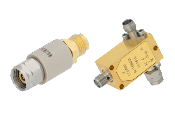
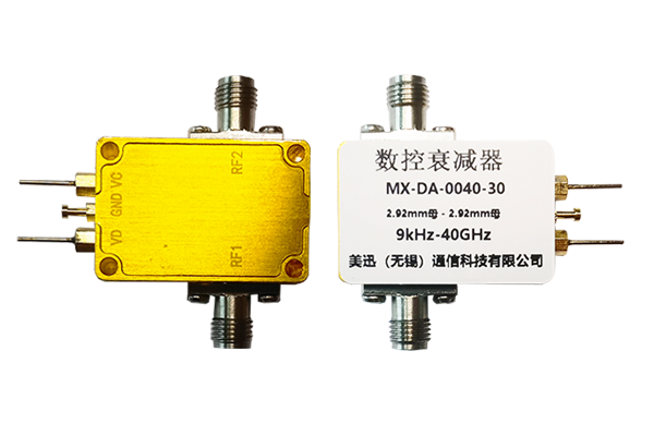
7. Use Matching Networks or Attenuators
- RF Matching Networks: Insert lumped-element (capacitor/inductor) or distributed-element (stub) networks between the switch and load to transform impedance to the desired value.
- Attenuators/Isolators: Place a fixed attenuator (e.g., 3–10 dB) or circulator between the switch and source to absorb reflections and improve mismatch tolerance.