

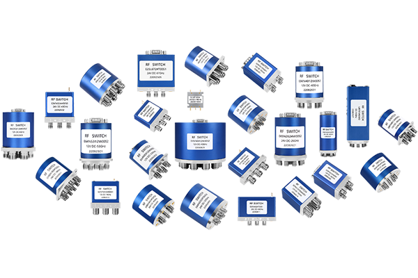


Evaluating the Power Handling Capability of PIN Diode Switches
The power handling capacity of a PIN diode switch is a critical parameter for RF and microwave applications, determining its ability to operate under high signal levels without degradation or failure. Below are the key factors and methods for assessment:
1. Key Parameters Affecting Power Handling
-
Peak Power (Pulsed Power)
-
Maximum instantaneous power the diode can withstand without breakdown (e.g., kW-level in radar pulses).
-
Limited by the diode’s reverse breakdown voltage (V_BR) and thermal dissipation.
-
-
Average Power (Continuous Wave, CW)
-
Sustained power the diode can handle without overheating (e.g., 10–100W for telecom applications).
-
Depends on thermal resistance (R_th) and heat sinking.
-
-
I-layer Thickness
-
Thicker I-layers (e.g., 50–100 µm) improve power handling but slow switching speed.
-
2. Evaluation Methods
-
Thermal Analysis
-
Measure junction temperature rise under load using infrared cameras or thermal simulations.
-
Ensure temperatures stay below 150–175°C (typical max for reliability).
-
-
RF Power Testing
-
Apply incremental power levels (CW/pulsed) while monitoring:
-
Insertion loss (should remain stable).
-
Harmonic distortion (indicates nonlinearity).
-
-
Failure signs: burnout, parameter drift, or increased VSWR.
-
-
Reverse Bias Leakage Current
-
High leakage under RF power suggests avalanche breakdown risk.
-
3. Practical Considerations
-
Duty Cycle: Pulsed systems allow higher peak power than CW.
-
Matching Circuits: Proper impedance matching reduces reflected power.
-
Heat Sinking: Active cooling extends power limits.
Applications:
-
High-power radar switches (e.g., T/R modules).
-
RF attenuators and limiter circuits.