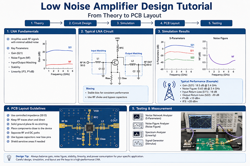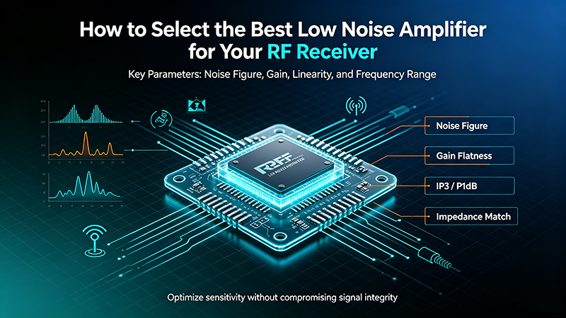


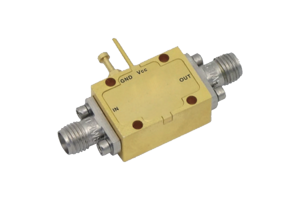
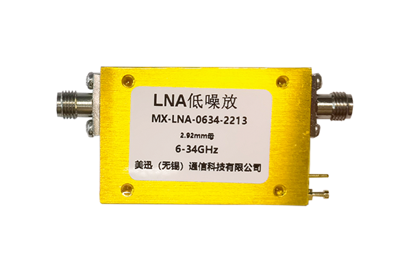




Low Noise Amplifiers are among the most critical components in RF and microwave systems, directly determining receiver sensitivity and overall system performance. However, designing high-performance LNAs presents numerous challenges that can lead to costly mistakes if not properly understood. This guide highlights the seven most common mistakes in LNA design and provides practical solutions to avoid them.
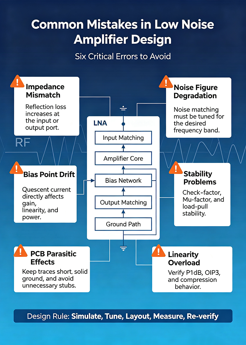
Improper Input Matching
One of the most fundamental mistakes in LNA design is matching the input for maximum power transfer instead of minimum noise figure. While conjugate matching maximizes power delivery, noise-optimized designs require matching to a different source impedance—the gamma-optimum point on the Smith chart.
Common Error
Designing input matching for 50-ohm conjugate match, resulting in higher than optimal noise figure. This approach prioritizes power transfer over noise performance.
Correct Approach
Match input to Gamma-opt (opt) for minimum NF. Accept slight VSWR penalty to achieve optimal noise performance. Use simulation to find the true optimum.
NF = NFmin + 4*Rn*|Gamma_s - Gamma_opt|^2 / |1 + Gamma_s|^2 / (Fmax^2)
How to Avoid This Mistake
- Always use noise parameters from the device datasheet or s-parameter files
- Run noise optimization in your simulator, not just gain optimization
- Verify that gamma-opt falls within a practical matching region
- Consider trade-offs between NF, gain, and VSWR
- Measure actual NF vs simulated to validate matching
Ignoring Stability Factors
Many LNA designs oscillate or exhibit marginal stability because engineers focus solely on gain and noise performance without thoroughly analyzing stability. Oscillations may not be obvious during testing but can cause intermodulation products, frequency pulling, and unpredictable behavior.
Common Error
Designing based on small-signal S-parameters without checking stability circles or Rollet stability factor (K). Marginal stability leads to oscillations under temperature or bias variations.
Correct Approach
Verify K > 1 and B > 0 for unconditional stability. Add stability networks if needed. Check stability across all bias points and temperatures.
K = (1 - |S11|^2 - |S22|^2 + |D|^2) / (2*|S12*S21|) where D = S11*S22 - S12*S21
Stability Enhancement Techniques
- Add series or shunt resistors at device ports (trade-off with NF and gain)
- Use RC networks at input/output for broadband stability
- Implement lossy matching networks
- Add gate-to-drain feedback (degenerate inductance)
- Use ferrite beads or lossy transmission line sections
Incorrect Biasing
Biasing mistakes can significantly degrade LNA performance or even damage the device. Common errors include improper gate voltage setting, insufficient drain current headroom, and neglecting bias circuit stability.
Common Error
Setting drain current arbitrarily without checking device datasheet recommendations. Operating too close to saturation or cutoff regions, causing poor linearity or insufficient gain.
Correct Approach
Select bias point for optimal NF and linearity trade-off. Ensure adequate drain-source voltage headroom. Use active bias circuits for temperature compensation.
Bias Circuit Best Practices
- Use self-bias or fixed-bias circuits appropriate for the device technology
- Implement temperature compensation to maintain consistent current over temperature
- Include RF chokes and bypass capacitors in bias networks
- Provide adequate decoupling to prevent RF feedback through bias lines
- Verify bias circuit stability under no-signal and large-signal conditions
Poor Thermal Management
LNA performance is highly temperature dependent, yet thermal considerations are often overlooked in the design phase. Excessive temperature degrades noise figure, reduces gain, shifts bias points, and can lead to thermal runaway in extreme cases.
Common Error
Designing for room temperature performance only. Ignoring thermal resistance from junction to ambient. Device heating causes NF degradation and potential reliability issues.
Correct Approach
Calculate expected junction temperature. Add thermal vias, heatsinks, or active cooling as needed. Design for stable operation across full temperature range.
Tj = Ta + (Pd * Rth_jc) + (Pd * Rth_cs) + (Pd * Rth_sa)
Thermal Design Guidelines
- Calculate total thermal resistance from junction to ambient
- Add copper ground plane area under and around the device
- Use thermal vias to conduct heat to internal ground planes
- Consider low-thermal-resistance packaging for high-power applications
- Implement temperature-compensated bias circuits
- Verify thermal performance with measurements at temperature extremes
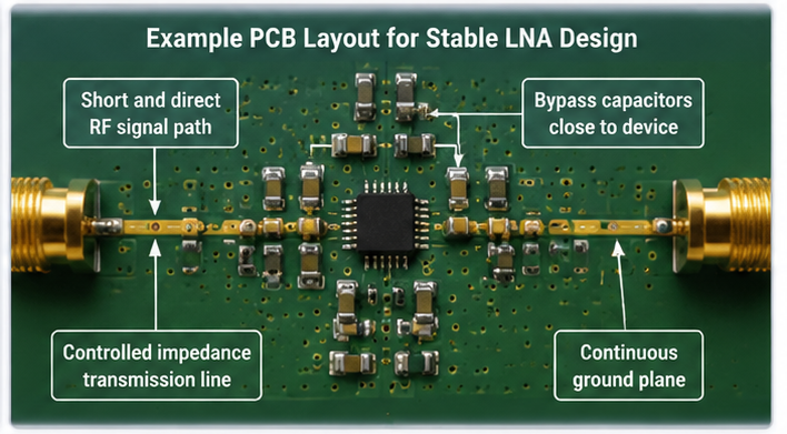
Neglecting Ground Layout
Inadequate grounding is one of the most common causes of LNA performance degradation and instability. Parasitic inductances and resistances in ground connections create feedback paths that affect gain, stability, and noise performance.
Common Error
Using single-point grounding or long ground traces. Via inductance creating ground loops. Insufficient ground plane under sensitive signal paths.
Correct Approach
Implement solid ground planes. Use multiple small vias instead of single large vias. Keep ground returns short and direct. Separate analog and digital grounds.
Grounding Best Practices for LNAs
- Use solid ground planes, especially beneath input and output traces
- Place vias close to device ground leads (within 0.5mm when possible)
- Use multiple small vias (0.3-0.5mm diameter) rather than single large vias
- Implement star grounding for bias circuits to avoid digital switching noise
- Keep input and output ground returns separate to prevent feedback
- Use coplanar waveguide with ground (CPWG) for controlled impedance and grounding
Improper Decoupling
Power supply noise and RF feedback through bias networks can significantly degrade LNA performance. Insufficient decoupling allows external signals to couple into the amplifier, causing intermodulation and reducing effective isolation.
Common Error
Using single decoupling capacitor or wrong capacitor values. Long supply traces introducing inductance. No isolation between stages in multi-stage amplifiers.
Correct Approach
Implement multi-stage decoupling with various capacitor values. Use chip inductors or ferrite beads for RF isolation. Keep decoupling network close to device pins.
f_SR = 1 / (2*pi*sqrt(L*C)) where L is package and trace inductance
Decoupling Network Design
- Use multiple capacitors in parallel (100pF, 1nF, 10nF, 10uF) for broadband decoupling
- Place smallest capacitors closest to device pins
- Use chip capacitors with low ESL and ESR for RF applications
- Add series inductors or ferrite beads for additional RF isolation
- Implement quarter-wave transmission line chokes for high-frequency biasing
- Separate bias networks between amplifier stages
Overlooking Package Effects
Device packages introduce parasitic inductances and capacitances that significantly affect high-frequency performance. Many designers rely solely on chip-level s-parameters without accounting for package models, leading to poor correlation between simulation and measurement.
Common Error
Using on-wafer s-parameters without package models. Ignoring bond wire inductance. Not considering lead frame parasitics at high frequencies.
Correct Approach
Request package s-parameters from manufacturer. Include bond wire models in simulation. Use chip-scale packages or die-level mounting for highest frequencies.
Package Parasitic Management
- Request complete package S-parameter models from the device manufacturer
- Model bond wire inductance (typically 0.5-2 nH per wire)
- Consider lead frame capacitance (0.1-0.5 pF typical)
- Use short bond wires, multiple wires in parallel when possible
- For frequencies above 10 GHz, consider chip-on-board or QFN packages
- Verify package model accuracy by comparing simulation to measurement
Summary: Avoiding the Seven Mistakes
Frequently Asked Questions
Conclusion
Designing high-performance Low Noise Amplifiers requires careful attention to multiple interrelated factors. By understanding and avoiding these seven common mistakes—improper input matching, ignoring stability, incorrect biasing, poor thermal management, neglecting ground layout, improper decoupling, and overlooking package effects—you can significantly improve your LNA designs.
Remember that LNA design is an iterative process. Start with proper matching for minimum noise figure, verify stability, then refine other parameters. Always validate your designs through simulation and measurement across the full operating temperature range.
The key to successful LNA design is understanding the trade-offs between noise figure, gain, stability, linearity, and power consumption. No single parameter should be optimized at the expense of others. A robust LNA design balances all these parameters while maintaining adequate margins for manufacturing variations and environmental conditions.
Need Expert Help with Your LNA Design?
Our RF engineering team can provide design review, optimization, and custom LNA development services to meet your specific requirements.
Contact Our Technical Team